At present, the automotive safety industry needs to reduce the number of components of small components, reduce the size and reduce the number of components, and promote semiconductor suppliers to add more power-consuming functions, resulting in higher component temperature, lower stability, and also affect car safety. By optimizing wafer configuration and power pulse time early in the design phase, designers can reduce the number of silicon tests and shorten development time. This article will first explain the function of the semiconductor thermal package, and how to use the model simulation software to assist the power supply components and system design, including the discussion of general automotive design challenges, model building techniques, thermal model verification and system upgrade.
The automotive electronics industry uses a variety of semiconductor packages ranging from small single-function transistors to complex power packages with more than 100 pins and special heat dissipation. The semiconductor package protects the die, provides electrical connections between the device and passive components external to the system, and manages heat dissipation. This article will discuss how semiconductor packages can dissipate heat from the wafer.
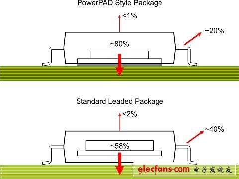
In a leaded package, the die attaches to the metal piece of the die pad. This die pad supports the die during construction and provides a good thermal conductor surface. In the automotive industry, the common type of semiconductor package is the exposed pad, which is the PowerPAD package. In this type of package, the bottom of the die pad is exposed and soldered directly to the printed circuit board (PCB), so that the die directly dissipates heat to the PCB, dissipates heat through the exposed pad soldered to the board, and then dissipates heat through the PCB. To the environment.
The exposed pad package can pass through the bottom and dissipate 80% of the heat into the PCB. The other 20% of the heat is dissipated from the device pins and the sides of the package. Less than 1% of the heat is emitted from the top of the unit.
The non-exposed pad package is also a pin package, but the die pad is completely covered by plastic and cannot be directly radiated to the PCB. In the standard pin package concept (see Figure 1), approximately 58% of the heat is dissipated from each side of the pin set package, 40% is dissipated from the bottom of the package, and approximately 2% is dissipated from the top of the package. Heat dissipation is performed by means of conduction, convection and radiation. For automotive semiconductor packages, heat dissipation is primarily transmitted to the PCB and convection to the surrounding air. Radiation accounts for a relatively small proportion of heat dissipation.

Figure 1. Heat sink and heat dissipation paths for standard pin packages and PowerPAD packages.
We are dedicated charging solution Manufacturer since 2005.
Supply various Power Station including Portable Power Stations, Solar Power Generators, Smallest Generator etc.
Manufacturing high quality products for customers according to international standards, such as CE ROHS FCC REACH UL SGS BQB etc.
To constantly offer clients more innovative products and better services is our consistent pursuit.
portable power stations for camping, solar pow er stations, jackery portable power station
TOPNOTCH INTERNATIONAL GROUP LIMITED , https://www.mic11.com