Abstract: A fast and effective method is proposed for the design of LDMOS wideband power amplifier matching circuit. After the initial value of the wideband matching circuit is obtained by multi-section parallel admittance matching method, the S parameters of the matching network are optimized by ADS software. The simulation results are as follows: In the frequency range of 1. 3 GH z~ 2. 3 GH z, the reflection coefficients of both ports are less than - 25 dB, and the transmission coefficient of the matching network is close to 0 dB. To achieve better impedance matching, ADS is used to optimize the matching network so that its impedance value is closer to the actual output impedance of the power transistor. This method is a good reference for designing broadband power amplifier matching circuits quickly and efficiently.
In addition to the military field, broadband power amplifiers have broad application prospects in the fields of wireless communication, mobile phones, satellite communication networks, global positioning systems, direct broadcast satellite reception, millimeter wave automatic collision avoidance systems, and optical transmission systems.
LDMOS power transistors have better thermal stability, frequency stability, better linearity, greater linear gain, higher efficiency and lower cross-modulation distortion than other microwave transistors. At the same time, LDMOS is based on mature silicon process devices, and the cost is much lower than other GaAs devices. Therefore, LDMOS is particularly suitable for power amplifiers in base stations of next-generation mobile communication systems.
Impedance matching is the key to the design of microwave power transistor amplifiers. A suitable impedance matching network can achieve the best power transfer efficiency in the passband. That is, the input impedance of the transistor amplifier is conjugate matched with the internal resistance of the signal source; the output impedance of the transistor amplifier is conjugate matched to the load impedance. The output impedance of the pre-stage transistor is conjugate matched to the input impedance of the post-stage transistor.
In the impedance-matched parallel admittance method, the impedance matching achieved is limited to a better match that can be achieved near the operating frequency. If the operating frequency changes, the input and output impedance (or admittance) of the microwave transistor will change accordingly. Therefore, to maintain a good conjugate matching in a wide operating frequency band, a multi-section parallel admittance matching method is used. The process is to describe the admittance values ​​measured by the transistors at different operating frequencies on the admittance chart, and the admittance values ​​are connected into a curve in order of frequency from low to high. In design, a plurality of parallel admittances are selected according to the curve, and are accessed from different positions to achieve conjugate matching in a wider frequency band.
Assuming that the distance between the parallel susceptor multiple access points and the transistor is 1, then at different operating frequencies, the transistor admittance values ​​are transferred along their respective VS coefficients to the number of wavelengths rotated by the parallel susceptance access point l / λ g Is different l / long < l / λ short. That is, in the entire operating frequency band, the admittance value of each point higher than the center frequency is larger than the number of wavelengths that the admittance value of each point lower than the center frequency travels along the respective equipotential wave coefficient circle moving distance. Thus, from one point on the microstrip line to another, the admittance value varies with wavelength as the original. This shows that the trajectory curve of the change of the admittance value of the transistor in the whole working frequency band is differently stretched at the high end and the low end of the band after accessing a microstrip line, thereby changing the admittance curve to the vicinity of the circle chart. Center, close to the matching point, to achieve the purpose of broadband matching.
1 Design ideasBecause the design method of the input-output matching circuit is similar, here, only the output matching circuit design of the LDMOS transistor amplifier MRF281Z is taken as an example. The initial value of the broadband impedance matching network is obtained by multi-section parallel admittance matching method, and combined with the method based on the moment method. The ADS software optimizes the target to quickly and efficiently achieve wideband impedance matching of transistor amplifiers.
2 load traction method to obtain output impedanceThe principle of the load pull method is to test the output power by continuously changing the load under large signal level excitation, and then draw the equal power and equal gain curves on the Sm ith impedance chart. This allows you to select the appropriate output impedance and accurately design the power amplifier to achieve the desired gain and output power.
Table 1 shows the optimum load impedance of the output impedance of the transistor MRF281Z at various frequencies from 1.4 GHz to 2. 2 GHz after being pulled by the ADS load.
Table 1 Output impedance of transistor MRF281Z

In order to deliver maximum power to the load or to place the microwave circuitry, transmission system in or near the traveling wave state, a conjugate matching network is required. The matching network has decisive constraints on the performance of the amplifier such as standing wave ratio, power gain, and output power.
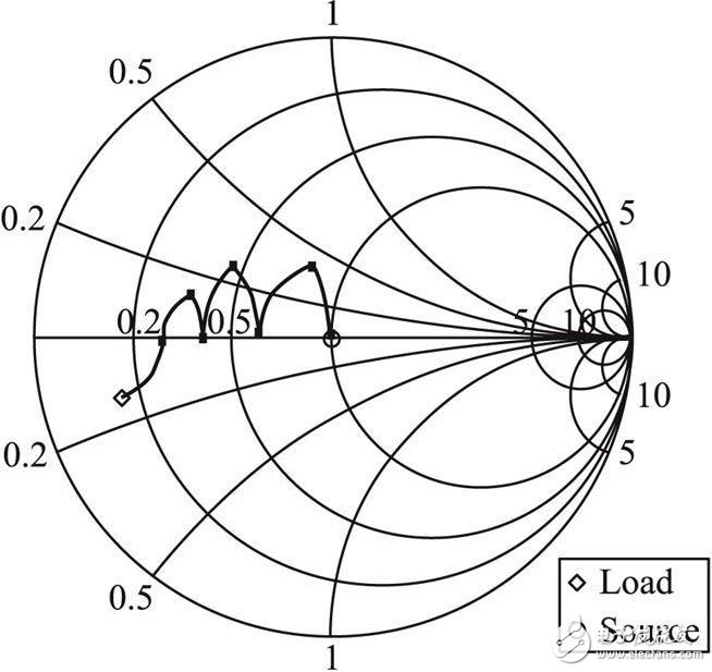
Under the condition of conjugate matching, the maximum transmission power is obtained. Here we take the output impedance of the frequency f = 1. 8 GHz Z out= 7. 807+ j 6. The conjugate impedance of 626 Z*out = 7. 807- j 6. 626 As the impedance of our matching port, four-strip microstrip line matching is performed in the Sm ith circle diagram using the conjugate matching method (as shown in Figure 1 and Figure 2).

Figure 1 Smith circle diagram for impedance matching with multi-section microstrip lines
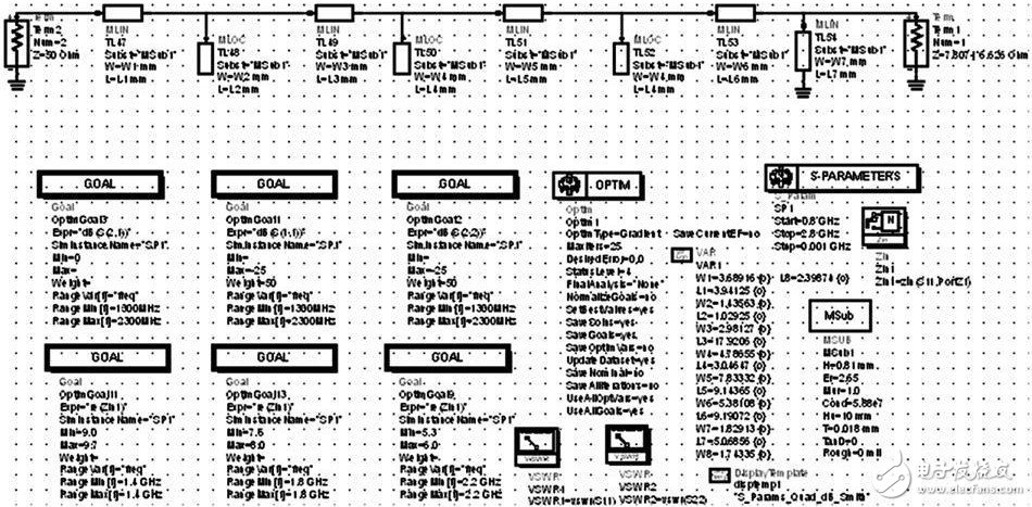
4 Simulation and optimization design with ADSThe matching circuit obtained above is simulated by ADS, and the length and width of each microstrip line are set as variables and optimized (as shown in Fig. 3). The steps are as follows:

Figure 3 Simulation and optimization of the output matching circuit with ADS
(1) Add the OPTIM control to the schematic:
Initial optimization with Random, and then partial optimization with Gradient.
(2) Add the optimization target GOAL control:
Here, we first optimize the S parameters of the matching network. The specific S parameter optimization target control configuration table is shown in Table 2.
Table 2 Optimized S-parameter target control configuration table

Laptop AC adapter for common brands, such as HP, Sony, Lenovo, Dell, Asus, Toshiba, Acer, Samsung etc. Our products have high quality and reasonable price.
CE, FCC, ROHS certification are approved by our products, and it have two years warranty. Built with input/output overvoltage protection, input/output overcurrent protection, over temperature protection, over power protection and short circuit protection. We are a professional power adapter manufacturer in China. We can meet your specific requirement. We have perfect after-sale service and technical support.
Hope we can establish friendly business relationship with you in the near future!
Laptop Adapter,Adapter For Macbook,Power Supply For Macbook, Charger For Macbook
Shenzhen Waweis Technology Co., Ltd. , https://www.huaweishiadapter.com