The anti-reverse protection circuit is designed by using the switching characteristics of the MOS tube and the conduction and disconnection of the control circuit. Since the internal resistance of the power MOS tube is small, the voltage drop and work of the existing diode power supply anti-reverse connection scheme are solved. Excessively expensive.
Anti-reverse protection circuit
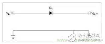
1. Under normal circumstances, the DC power input anti-reverse protection circuit uses the unidirectional conductivity of the diode to achieve anti-reverse protection. As shown in Figure 1 below:
This connection is simple and reliable, but the power consumption is very large when a large current is input. With the input current rating up to 2A, if Onsemi's fast recovery diode MUR3020PT is used, the rated tube voltage drop is 0.7V, then the power consumption must be at least: Pd=2A&TImes; 0.7V=1.4W, so the efficiency is low and the heat is large. , to add a radiator.
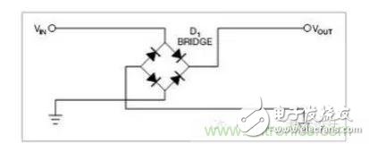
2. In addition, the input can be rectified with a diode bridge so that the circuit will always have the correct polarity (Figure 2). The disadvantage of these solutions is that the voltage drop across the diode consumes energy. When the input current is 2A, the circuit consumption in Figure 1 is 1.4W, and the power consumption of the circuit in Figure 2 is 2.8W.

Figure 1. A series diode protection system is unaffected by reverse polarity. The diode has a voltage drop of 0.7V.

Figure 2 shows a bridge rectifier that works fine regardless of polarity, but with two diodes turned on, the power consumption is twice that of Figure 1.
The anti-reverse protection circuit is designed by using the switching characteristics of the MOS tube and the conduction and disconnection of the control circuit. Since the internal resistance of the power MOS tube is small, the voltage drop and work of the existing diode power supply anti-reverse connection scheme are solved. Excessively expensive.
MOS tube type anti-reverse protection circuitFigure 3 utilizes the switching characteristics of the MOS transistor, and the control circuit is turned on and off to design an anti-reverse protection circuit. Since the internal resistance of the power MOS transistor is small, the MOSFET Rds(on) can now be implemented in milliohms. It solves the problem of excessive voltage drop and excessive power consumption in the existing diode power supply anti-reverse connection scheme.
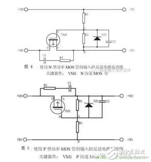
The reverse polarity protection protects the FET from being connected in series with the protected circuit. The protection field effect transistor is a PMOS field effect transistor or an NMOS field effect transistor. In the case of a PMOS, its gate and source are respectively connected to the ground and power terminals of the protected circuit, and the drain thereof is connected to the substrate of the PMOS device in the protected circuit. In the case of an NMOS, the gate and the source are respectively connected to the power supply terminal and the ground terminal of the protected circuit, and the drain thereof is connected to the substrate of the NMOS device in the protection circuit. Once the polarity of the power supply of the protected circuit is reversed, the protection field effect transistor will form an open circuit to prevent the current from burning the FET component in the circuit and protecting the overall circuit.
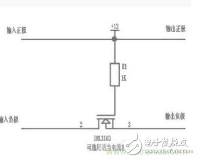
The specific N-channel MOS tube anti-reverse protection circuit is shown in Figure 3.

Figure 3. NMOS tube type anti-reverse protection circuit
The N-channel MOS transistor is connected in series between the power supply and the load through the S pin and the D pin. The resistor R1 provides a voltage offset for the MOS transistor, and the switching characteristics of the MOS transistor are used to control the conduction and disconnection of the circuit, thereby preventing the power supply. Reversed to damage the load. In the positive connection, R1 provides the VGS voltage and the MOS is saturated. When the reverse connection, MOS can not be turned on, so it plays a role of anti-reverse connection. The Rds(on) of the power MOS transistor is only 20mΩ, the actual loss is very small, the current of 2A, the power consumption is (2&TImes; 2) & TImes; 0.02=0.08W, no external heat sink is needed. It solves the problem of excessive voltage drop and excessive power consumption in the existing diode power supply anti-reverse connection scheme.

VZ1 is a Zener diode to prevent the gate-source voltage from being too high to break through the mos tube. The on-resistance of the NMOS transistor is smaller than that of the PMOS, and it is preferable to select an NMOS.
The NMOS transistor is connected to the negative terminal of the power supply, and the gate is turned on at a high level.
The PMOS transistor is connected to the positive terminal of the power supply, and the gate is turned on at a low level.
Linear Power Supply,12V Linear Power Supply,24W Linear Power Supply,15V Linear Power Supply
Guang Er Zhong(Zhaoqing)Electronics Co., Ltd , https://www.cnadaptor.com