Introduction For all types of M CUs (microcontrollers), the power supply is not only used to supply power, but also to ensure the accuracy of its reference source. After power-off, the MCU will stop working, clock stop, RAM (random access memory) data loss and other adverse consequences, so the high reliability of the power supply itself must be guaranteed. The power-down protection circuit can be said to be numerous, but the circuit that is suitable for the whole machine and cost-effective and easy to mass-produce should be the goal pursued by engineers.
1 Scheme selection
In combination with the requirements of Q/GDW1364-2013 single-phase smart meter technical specification, we designed a single-phase cost-controlled smart energy meter power supply. In addition to meeting the general requirements of the power supply, the power supply also requires small size, low power consumption, high cost performance, and three-way transmission.
Out (13V/2W pull-and-close power supply,
1 2 . 4 V / 1 . 5 W carrier interface power supply and 5 V / 0. 3 W M CU power supply) The grounding and carrier interface power supply (hereinafter referred to as V 1 2 ) shall not affect the normal operation of the pull-close power supply (hereinafter referred to as V13) and the MCU power supply (hereinafter referred to as V05) when short-circuited. Due to the limitation of volume, the scheme of adopting pure linear power supply is first eliminated, and the scheme of using three windings, rectification and wave-wave of pure switching power supply is excluded. Among the three outputs, the most important of course is the MCU power supply V05, followed by the pull-close power supply V13, and the carrier interface power supply V12 is relatively speaking.
The requirements are lower, and according to this we use a switching power supply and a linear hybrid solution.
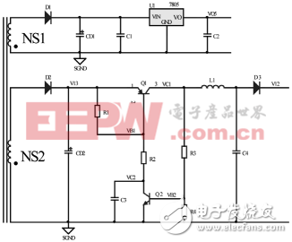
Figure 1 Hybrid power scheme (V13 voltage feedback section omitted)
2 program optimization
The hybrid scheme is such that: V05 is an output winding of the switching power supply, which is regulated by diode half-wave rectification, capacitor filtering and three-terminal regulator LM7805 to obtain a stable output; V13 is another output winding of the switching power supply, through the diode Half-wave rectification, capacitor filtering and secondary voltage feedback provide a stable output; V12 takes V13 as the input, and uses a transistor regulator circuit to obtain a relatively stable output, as shown in Figure 1.
After testing, the output of each channel meets the requirements when static. However, when V12 is short-circuited, V13 and V05 have severe power-down, as shown in Figures 2 and 3.
It can be seen from Fig. 2 that the time from V1 to the normal voltage is reduced to 48.8ms, which is not allowed for the pull-in power supply. As can be seen from Figure 3, the V05 is from the power-down to the normal voltage recovery time of 96ms, which is intolerable for the MCU power supply.
3 machine debugging
The following is a theoretical analysis of Figure 1: When static, the transistor Q2 is turned on, VC2 is grounded, and VB1 is clamped by the transistor Q1 that is turned on. When V12 is short-circuited, the base voltage VB2 of transistor Q2 is low due to the voltage division of resistor R3 and resistor R4, which is insufficient to turn Q2 on. After Q2 is turned off, the electrolytic capacitor CD2 starts to charge the capacitor C3 through the resistor R1 and the resistor R2, and the CD2 itself is also discharged. When the VB1 is charged to a certain voltage value, the transistor Q1 is turned off. Thereafter, even if the V12 short-circuit state is not released, V13 remains at the normal voltage value (13V). It can be imagined that if the charging can be accelerated, the voltage of the electrolytic capacitor CD2 has not decreased or decreased, and the falling time is not long.
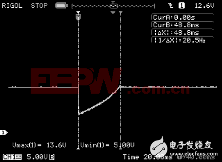
Figure 2 V13 waveform when V12 is shorted
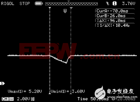
Figure 3 V05 waveform when V12 is shorted
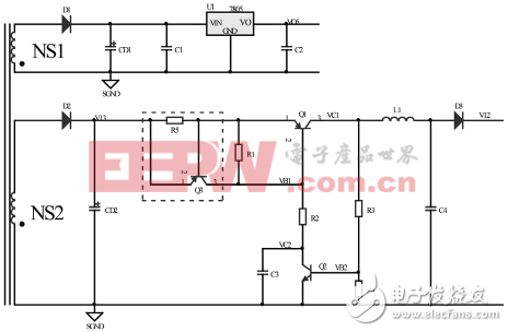
Figure 4 Adding a hybrid power supply scheme after accelerating the charging circuit
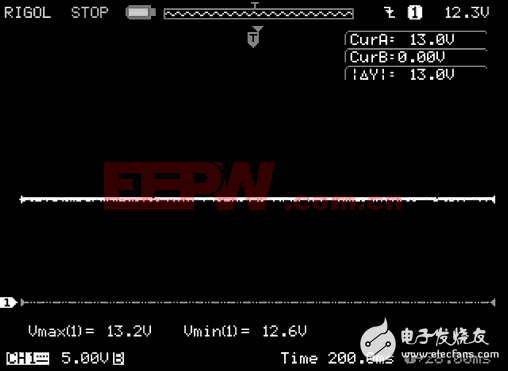
Figure 5 Waveform of V13 when V12 is short-circuited after adding a fast charging circuit
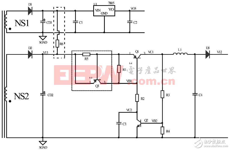
Figure 6 Hybrid power scheme after adding temporary power supply circuit
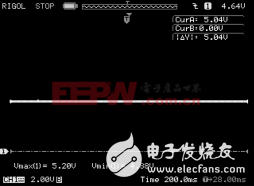
Figure 7 Waveform of V05 when V12 is short-circuited after adding temporary power supply circuit
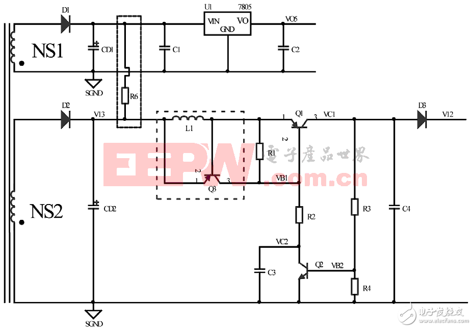
Figure 8 Final hybrid power scheme after improving the acceleration charging circuit
V13 does not lose power. To this end, a fast charging circuit is added to the circuit, as shown by the dashed box in FIG. After testing, when V12 is short-circuited, V13 will no longer be powered down, as shown in Figure 5. As can be seen from Figure 5, the power down problem of V13 is solved. However, the power failure of the V05 has not been resolved. As can be seen from Figure 3, V05 takes 96ms from power-down to normal voltage recovery.
If there is a temporary stable and reliable power supply to the three-terminal regulator U1 (7805) during this time, then V05 should be
It will not be powered down. Wait until the voltage at the input of U1 returns to normal and then cut or clamp the temporary power supply. To this end, a temporary power supply circuit is added, as shown by the dashed box in FIG.
After testing, when V 1 2 is short-circuited, V05 will no longer be powered down, as shown in Figure 7. It can be seen from Fig. 7 that the power failure problem of V 0 5 is also solved. After further researching the power-down protection circuit, it was found that there are still improvements. The resistance of the resistor R5 is 2 ohms, and the ESR (equivalent series resistance) of the inductor L1 is 1.7 ohms. L1 is used as the filter inductor. It should be possible to connect it in series elsewhere in the bus. In this case, if L1 is placed at R5, L1 still acts as a filter, and its equivalent series resistance should act as resistor R5. 8 dotted line box
Show. After testing, when V12 is short circuited, the power failure problem of V13 and V05 can still be solved. It should be pointed out that moving L1 to R5 seems to be a no-brainer. There is no high-tech content. In fact, this move has the following advantages:
1 Save one material, saving material cost and management cost;
2 Saves two solder joints, saving processing costs;
3 saves a certain amount of space, reduces LAYOUT (layout) and
Difficulty of ROUTE (wiring);
4 AXIAL package inductors are easier to dissipate heat and withstand than chip resistors
hit;
5 Reduce the power consumption of the whole machine
4 Design Summary
The final hybrid power supply scheme (shown in Figure 8), taking into account the requirements of the Q / GDW1364-2013 single-phase smart meter technical specification and the characteristics of the power supply product itself, clever use of common components under limited conditions
(Triode, inductor and resistor), achieving cost-effective power-down protection. In addition, this power-down protection circuit has considerable practical value from the perspectives of material procurement, production processing, and heat dissipation.
Starting System,Starting Air System,Engine Starting System,Stop And Start Engine System
Chongqing LDJM Engine Parts Center , https://www.ckcummins.com