On May 25-27 this year, the first Asian Consumer Electronics Show will be held at the Shanghai New International Expo Center in Shanghai to showcase the latest electronic products and hi-tech technologies that will enter the Asian market. The exhibition was sponsored by the Consumer Electronics Manufacturers Association of the United States (CEA). The three themes of the show were: "Connectivity," "Innovation," and "Internet of Things." IBM, the industry giant, attacked CES Asia and displayed IBM's technologies and achievements in the frontier areas of the Internet of Things, cloud computing, big data analysis, and mobile computing.
During the exhibition, Mr. Qian Daqun, Chief Executive Officer of IBM Greater China, delivered a keynote entitled "Creating Unbounded Potentials" and shared IBM's insights, strategies, and important cooperation and results on the Internet of Things. In addition, IBM held the "Data Wisdom Empowering IoT - IBM IoT Media Conference" during the exhibition. IoT experts from IBM shared with guests IBM's government, electronics, automotive, energy manufacturing, and retail sales. Successful Internet of Things practices in communications, healthcare, and other areas.

Mr. Qian Daqun, Chief Executive Officer of IBM Greater China
In the keynote speech, Mr. Qian Daqun, Chief Executive Officer of IBM Greater China, said: "IBM recently announced investment of 3 billion US dollars to build a new Internet of Things (IoT) business unit, highlighting our entry into the Internet of Things and big data analysis Our belief is that the Internet of Things will make our lives better and safer, the environment will be cleaner, entertainment will be more colorful, and our lives will be healthier. This is a wonderful time, and the Internet of Things is just getting started and is far from mature. It is the top priority for customers to bring in the products and services they want.As a leader in information technology, IBM will use its deep understanding of the industry to advance the Internet of Things with the most advanced analytical technologies. Together to create a smart world."
Create Experience, Promote Change, Big Data Become the Core Driver of Internet of Things
The Internet of Things is the core application technology that promotes the "Made in China 2025" and "Internet +" strategy. The real value comes from the analysis of the massive data on the Internet of Things. Therefore, data analysis will give the true power of the Internet of Things. The Internet of Things driven by big data is the valuable Internet of Things.

Dr. Shen Xiaowei, President of IBM China Research Institute
Dr. Shen Xiaowei, President of IBM China Research Institute, said: “We are moving towards the Internet of Things (IoT) 3.0. This phase is the most different from the previous Internet of Things. It is the deep integration of IoT technology and cloud computing technology, and data analysis technology. The development will have a huge impact on the Internet of Things."

Scott Burnett, IBM Global Consumer Electronics Industry Director
Scott Burnett, director of IBM’s global consumer electronics industry, pointed out: “According to IBM’s statistics, there are already more than 9 billion connected devices in the world today, and 90% of the data generated from multiple devices has never been analyzed or taken any measures. Up to 60% of the data starts to lose value within a few milliseconds of its generation, and today, IBM's cloud computing and big data analytics technologies are bringing vitality and value to the Internet of Things, which in turn drives innovation, transformation and transformation in the industry. â€
Increase investment + co-creation with enterprises, IBM launched the Internet of Things
As one of the important strategic development directions of IBM in the recent past, from the global layout to the deep-growing hot-spot industry market, IBM's two levels go hand in hand and launch the Internet of Things. On one hand, IBM recently announced that it will invest US$3 billion in the next four years to build a new Internet of Things (IoT) business unit and will launch a series of solutions for corporate Internet of Things applications. It is worth mentioning that IBM recently announced the establishment of a new global strategic partnership with WSI, a subsidiary of The Weather Company, which will help various industries use insights about the impact of weather on the business in their operations.

On the other hand, IBM is launching more and more successful IoT industry applications. During the conference, experts from IBM Global Business Consulting Services shared with guests the successful practices of IBM in government, electronics, automotive, energy manufacturing, retail, communications, healthcare, and other areas: Green Horizon can Predicting high-precision air quality through weather and air monitoring sensors to guide industrial production and people's lives; IBM assists Futian Lovol, the largest agricultural equipment manufacturer in China, to create a marketing and after-sales service system based on the Internet of Vehicles model to comprehensively enhance R&D and production Capability; IBM and Apple team up to improve the quality of life of millions of Japanese elderly people. Through Apple’s mobile smart devices iPads and IBM’s application and data analysis technologies, millions of elderly people are provided with medical and other services to assist them and the community. Family communication.

Wang Tao, general manager of the automotive and industrial products industry at IBM Global Business Services, said: “China has clearly established a national strategic plan for the development of China for 2025, pointing out the direction and concrete implementation path for China’s transformation from a manufacturing country to a manufacturing powerhouse. With the concept of "Made with China", IBM has taken a global perspective, based on its own transformational experience, rich industry experience and resources, and leveraged the Internet of Things, cloud computing, big data, mobile social technology, and China. Manufacturing companies jointly promote industrial innovation and upgrades."

Chen Huaiyu, general manager of IBM's Greater China electronics industry, said: "The data-centric Internet of Things is entering our lives. More and more electronics manufacturing companies are using IBM's data analysis capabilities for smart homes, wearable devices, etc. Massive data is analyzed and excavated to gain insight into consumer demand, and this insight is reflected in product development, design, production, marketing, and even in the entire process of business operations, while enhancing the consumer experience while realizing its own products and Service model innovation."

For more information, please click to enter the CES2015 in Asia
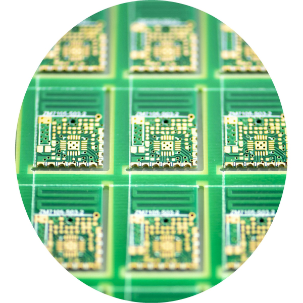
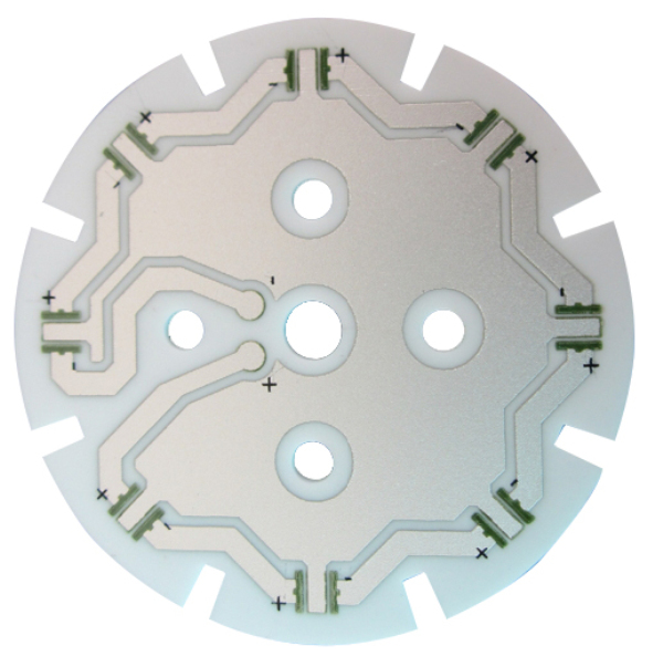
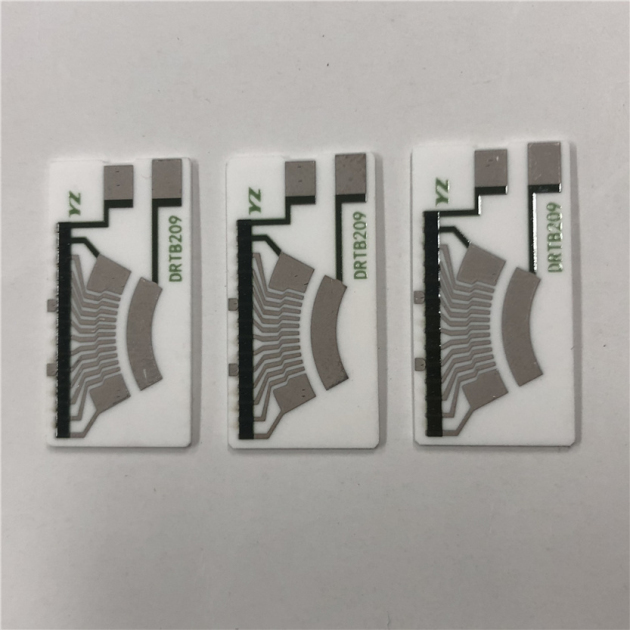
How are ceramic PCBs made?
With the emerging demand for durable, reliable miniature, high-density, high-power, and precision electronic devices, there has been a range of improvements in the design and development of these electronic devices. Therefore, engineers have conducted research in various fields of electronics, especially in the field of semiconductor electronics and printed circuit boards (PCB), integrating more electronic products into an Originality Electronics IC package. Therefore, we know the emergence of LSI and VLSI technologies, which integrate thousands of electronic circuits or gates in a single integrated circuit (originality electronics IC) package. With the passage of time, this technology has been greatly developed, and now it is necessary to improve the PCB on which these semiconductor ICs will be mounted. Therefore, designers proposed blind via hole (blind via hole PCB), buried via (buried PCB), via pad technology solutions, and introduced many other technologies to achieve high-density interconnect HDI PCB. As the density increases, power consumption also increases, thereby generating more heat. Therefore, ordinary FR-4-based substrate PCBs cannot withstand such high temperatures, and the thermal characteristics of FR-4 are not up to standard, so researchers have found a solution in the form of "ceramic substrate printed board".

1- extraordinary thermal conductivity
2- Good mechanical strength
3- High-density interconnection (HDI) is easy to implement on ceramic PCB
4- Compatibility of CTE with conductive layer, wiring and components.
5- Chemical resistance
6-Provide better high frequency performance
7-The coefficient of thermal expansion (CTE) value is low
8- can be packed in a waterproof sealed package
9- Reduce the system cost in general, especially the front-intensive packaging
10- No need for surface treatment like OSP or HASL
11-The traces can be printed with silver and protected with glass. If corrosion is a problem due to environmental conditions, gold plating can be used to protect the exposed silver pad
12-The thermal conductivity of some ceramic materials is

High temperature co-fired ceramic (HTCC) PCB:
The main components of HTCC ceramic substrates are alumina, plasticizers, binders, lubricants and solvents. The mixture will form a raw ceramic, which is then calendered and curtain coated. Tungsten or molybdenum can be used as the metal for circuit printing. Next, it was exposed to a high temperature of 1700 O C and baked in hydrogen for 32 to 48 hours. Then it is laminated and cut. This is suitable for small-sized ceramic plates, and is not suitable for large-sized ceramic plates due to inappropriate shrinkage tolerances and poor warpage
Low temperature co-fired ceramic (LTCC) PCB:
This is a combination of glass crystals and glass composite materials. In addition, other ingredients are added, such as adhesives and non-glass ingredients. Then, high-conductivity gold paste is used to create circuit traces, and then processed/baked in an oxidizing gas furnace at a high temperature of 900 O C.

Here, two alternating thick films are applied on the ceramic substrate. One is gold thick film and the other is dielectric thick film. However, because gold is expensive, copper thick film is implemented, which is a recognized technology for ceramic PCBs. The stack is then moved into a filled baking furnace (to avoid oxidation of copper), in which it is processed at a temperature of 1,000 °C in nitrogen. The dielectric paste is produced by nitrogen.
Application of ceramic PCB:
1-High-current high-brightness LED lights and spotlights.
2-Automotive electronic equipment, such as power controllers, optical systems, power converters and power conditioners
3-Industrial power equipment, such as servo drives, robots, etc.
4- Microprocessor, graphics card and IC array
5-semiconductor device
6-Audio power amplifier based on high power transistor
7-Solar battery related circuits, inverters, chargers, etc.
8- DC-DC regulator and power management circuit, etc.
Ceramic Printed Circuit Boards,Flame Resistant Pcbs,Fr-4 Pcb Laminate,Fr4 Pcb Boards
HAODA ELECTRONIC CO.,LIMITED , https://www.pcbhdi.com