Design of Current-Fieldbus Conversion Instrument Based on WORLDFIP
Discuss the development of current-fieldbus converter based on WorldFIP fieldbus protocol. The principle and specific design of the current-field bus converter are specifically introduced from two aspects of hardware design and software development.
Keywords: converter; protocol; FOUNDATION fieldbus
Design for the Converter of Analog to Fieldbus Based on WORL DFIP
LI Wen, BAIYan, LIANGGeng?
(AutomaTIon Department of North Electric Power University, Beijing 10 2206, China)?
Keywords: converter; protocol; FF
1 Hardware design The current / bus converter (IF) is mainly composed of three modules: input module, communication module and display module, as shown in Figure 1. On the input circuit board, the 4-20mA standard signal from the conventional instrument is adjusted to a voltage suitable for A / D conversion after signal adjustment. After the signal is isolated, it is sent to the field bus and application in the form of digital quantity through the communication board The layer communicates, and at the same time converts the digital signal into a numerical display of actual physical quantities.
1.1 The input module is shown in Figure 2. In order to save costs and fully improve the conversion efficiency of the IF, the IF is designed to have four input conversion channels. The function of connecting a resistor to each input end is to multiply the input signal with a correct gain to suit the signal reception range of the A / D converter. The input is an analog signal of 4 ~ 20mA. After a resistance of R = 100Ω, the signal entering the A / D converter is a voltage signal of 0.4 ~ 2V (the standard voltage of ADS1110 is 2.048V).
1.1 The input module is shown in Figure 2. In order to save costs and fully improve the conversion efficiency of the IF, the IF is designed to have four input conversion channels. The function of connecting a resistor to each input end is to multiply the input signal with a correct gain to suit the signal reception range of the A / D converter. The input is an analog signal of 4 ~ 20mA. After a resistance of R = 100Ω, the signal entering the A / D converter is a voltage signal of 0.4 ~ 2V (the standard voltage of ADS1110 is 2.048V).


The main function of the A / D conversion circuit is to perform A / D conversion on the amplified signal. The A / D converter uses ADS1110. The chip mainly has the following advantages: the resolution is 16 bits, thus ensuring a high accuracy of A / D conversion; on-chip 2.048V standard reference voltage, the accuracy is 2.048V ± 0.05%; with 8-bit I2C address line, Serial output reduces the use of photoelectric isolation components. In addition, the A / D converter is also equipped with zero adjustment and gain calibration circuits.
The role of power isolation and signal isolation is to prevent the input signal from forming a loop with ground and introducing interference. The control signal from the CPU of the main circuit board and the signal from the A / D converter are transmitted through the photocoupler, thereby realizing the isolation of the signal ground.
The central processing unit CPU is the core component of the current-field bus, which controls the coordination, linearization and communication of the various components of the entire instrument. The CPU uses AT91M40800. The chip integrates ARM7TDMI core, with high-performance 32-bit RISC; on-chip SRAM and ROM; 4G linear address space, 32-bit programmable I / O lines and other characteristics. In addition, the on-chip JTAG debugging port of this series of single chip can be emulated online. The system program is stored in the PROM outside the CPU, the operation data is temporarily stored in the RAM, and some important application programs such as calibration, configuration and identification are stored in the EEPROM. The EEPROM memory on the main circuit board is used to store the configuration parameters (referring to the parameters of the function module).
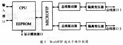
1.2 WorldFIP communication module In the design of the communication module, the communication unit adopts the WorldFIP communication microcontroller MICROFIP designed by ALSTOM, and the communication interface part uses the WorldFIP bus driver FIELDDRIVE and WorldFIP isolation transformer F IELDTR designed by ALSTOM. The composition block diagram of the communication card is shown in Figure 3. ?

MICROFIP provides the interface between the data link layer and the MPS application layer. The services provided are:
1) Physical layer service: choose between EN10570 and FIP standards; 2) Data link layer service: variable transmission service and message transmission service; 3) network management service: MICROFIP media redundancy management; 4) additional functions: Input / output port, get the station address through the parallel port.
FIELDRIVE components are a set of fully integrated bus driver circuits used to provide the interface between protocol components and field bus isolation transformers. It integrates a bus driver, a bus receiver, a set of transmission error detection circuits, a monitoring interface . The FIELDTR element provides electrical isolation between the FIELDDRIVE bus driver and the physical media of the fieldbus.
1.3 The display panel uses the character LCD dot matrix module HD44780, which can display 5 × 7 dot font 192 characters, 5 × 10 dot font 32 characters, and can be self-programmed 8 (5 × 7 dots) or 4 (5 × 10 dots) ) Kinds of characters. The command function of this module is strong, and can be combined into various input, display, shift modes to meet different requirements. The interface has 8 × 8bitRAM. ?
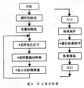
Software development uses an integrated development environment-Enbest IDE for ARM. It can provide an efficient and clear graphical embedded software platform, including a complete set of development and debugging tools for embedded systems. IF software design also adopts the modular design idea, and divides the software design into three modules: A / D conversion module, communication module and display module. The A / D conversion module mainly collects the input signal of the required channel (converted into digital quantity). The communication module is the core module that all field bus intelligent instruments must have. It completes the communication between the physical layer and part of the data link layer, and realizes the communication between the field device nodes and the field bus. The display module is mainly responsible for displaying the actual physical quantity. The digital quantity after A / D conversion is scaled to obtain the actual value displayed. The main program block diagram is shown in Figure 4.
 ?
? The superiority of the fieldbus control system is indisputable, therefore, fieldbus intelligent instruments similar to current-fieldbus converters have a wide range of application prospects. For large-scale industrial control systems similar to thermal power plants, most of which are still using DCS control systems, if they are transformed into field bus control systems, it is necessary to build a bridge between conventional instruments and field bus The development of current-fieldbus converters and fieldbus-current converters has enabled the fieldbus control system to penetrate into various control fields and created a new era of industrial control.
Nantong Boxin Electronic Technology Co., Ltd. , https://www.bosencontrols.com