 The last day of IDF is Intel's future prospect show. CTO Justin Rattner also announced that Intel will jointly develop a new DRAM technology with Micron, named "Hybrid Memory Cube" (HMC), aiming for future memory in the process of CPU development. The bandwidth bottleneck gives a solution. Ten years ago, we used DDR SDRAM to give a more economical solution to RDRAM, which increased the memory bandwidth to 128 bits, but the frequency of DDR memory cannot be increased indefinitely, so this method will increase the memory bandwidth. The more difficult it is.
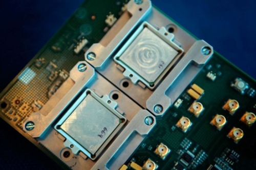
 Intel and Micron's idea is to stack multiple DRAM chips together, and use a logic processing layer (CPU processing sense, not DRAM manufacturing layer) to buffer and route, so that the total bandwidth of DRAM is extremely high. Large increase in power consumption remains almost unchanged. This logic processing layer is the key to this "sandwich" type memory, solving a very important problem of stacking multi-layer chips: how to "connect" the pins to each layer. This logic routing layer hybrid DRAM technology naturally named "Hybrid Memory Cube."
The HMC technology co-developed by the two companies can now be compared with the low-voltage DDR3. With almost the same energy consumption, the bandwidth can reach over 1Tbit/s, and the efficiency is 7 times that of the original. But the biggest problem at the moment is the production of packaging, but I believe that the industry will naturally come up with solutions when it is necessary.
TOPCOM Lighting Co., Ltd. , http://www.lightingifts.com