The white LED driver provides a cost-effective option for driving a power-constrained xenon flash to illuminate the scene. This article describes the basic concepts of xenon lamps and details a typical low-power, low-cost flash drive circuit design based on ON Semiconductor's NCP5007 chip.
Digital cameras and mobile phones with camera functions have changed from new products to mainstream products. The digital image sensors inside these products are based on CCD or CMOS technology. In order to support image sensors in the absence of light, flash circuits have become a necessary solution for digital cameras and are becoming more common in camera phones. The main sources of light that meet flash requirements are xenon bulbs and now emerging high-brightness white LEDs.
The main advantage of xenon lamps is the high power light output produced by the flash pulse, while the LED solution has the advantage of being relatively small and thin, and can be turned on for longer periods of time in video capture, although its light output is only moderate compared to xenon lamps. In particular, the xenon lamp provides a very short flash pulse that allows the camera to capture a still picture. They require special drivers to generate high voltage and large storage capacitors to store electrical energy.
We have found that white LED drivers provide a cost-effective option for driving power-constrained xenon flashes to illuminate the scene. This article describes the basic concepts of xenon lamps and details a typical low power/low cost flash application.
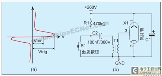
Figure 1: (a) Xenon flash breakdown voltage.
(b) Basic flash light.
Xenon lamp concept
The xenon lamp has a glass envelope with an electrode at each end filled with a low pressure rare gas mixture. In steady state, as shown in Figure 1, the voltage on the electrode is set to be lower than the trigger voltage. At this point no current flows and the system remains stable until a trigger voltage is applied across the third electrode. For the low power lamp under consideration, this high voltage pulse is in the range of 1 kV, which comes from a transformer with a small core and is triggered by a sudden discharge of capacitor C2 (see Figure 2).
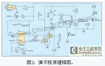
Figure 2: Block diagram of the demo board.
When the gas mixture is excited, the plasma produces a flash of light. For consumer applications, the typical duration of the flash is 2ms. Depending on the type of flash associated, the energy stored in capacitor C1 can be as low as 1 joule (small camera) or as high as several kilojoules (professional application). The energy consumed by the flash is shown in Equation 1:

The capacitor charging voltage is basically 160V to 600V depending on the type of xenon lamp used. Low-power handheld cameras require no more than a few joules of energy and an output voltage range of 160 to 250V. Higher voltages are generally seen in devices used in professional studios.
In addition to the DC voltage, a high voltage pulse must be provided to excite the plasma in the bulb, creating a high intensity arc between the electrodes at both ends. The pulse amplitude depends on the type of bulb used in the system, ranging from a lower 1.6kV to more than 10kV. The miniature xenon lamp is triggered by a 1.6 kV/5 μs pulse applied to the third external electrode of the lamp, which pulse is generated by a dedicated pulse transformer as shown in Figure 2 connected to a high voltage capacitor. The capacitor is charged to the flash DC voltage (200V) and suddenly discharges to the primary side of the pulse transformer after the trigger button S1. A high voltage from the secondary side is applied to the bulb (on the outer surface) and the flash is activated.
The main advantage of this concept is that the light output is large and the pulse duration is very short, allowing fast-moving photos to freeze the moving subject at a certain point. The disadvantage of this design is that the size of the storage capacitor is large, requiring a higher voltage on the board, and the capacitor needs to be recharged during shooting (the charging time for consumer applications is 5 to 10 seconds).
Depending on the sensitivity of the imager and the aperture of the lens, in the general environment of consumer applications, a relatively small capacitance is sufficient to take a bright picture. Therefore, a simple converter can be used to boost the battery voltage to the 200V required for a low voltage xenon lamp.
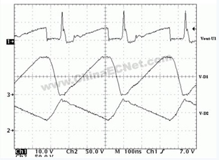
Figure 3: Primary and secondary output voltage waveforms.
Low power flash converter
The low-power flash converter described in this article is based on the ON Semiconductor NCP5007 chip. The chip was originally developed to drive white LEDs in series. In this application, the main consideration is the voltage limit associated with up to 28V silicon breakdown. To overcome this challenge, an external transistor can be used, which can hold a minimum of 250V, or a transformer with a primary to secondary ratio of 1:10.
Assuming a storage capacitor of 50μF, the operating voltage of a small xenon lamp is 200V, and the energy of the flash is:
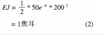
This energy is transferred from the battery to the storage capacitor by a boost converter constructed using a DC/DC converter. Although the structure of the NCP5007 is based on the flyback mode, it cannot be used directly because the chip operates in pulse frequency mode (PFM), and the time parameters are variable Ton and a constant Toff maximum of 300 ns. Therefore, if a conventional flyback topology is used, the secondary inductor will not fully discharge during the Toff time, and the core will quickly saturate, producing very small inductance and low energy transfer at the primary side.
To overcome this limitation, a combined approach is to combine the flyback and forward modes to increase the output voltage capability. This combination is obtained by four diodes packaged in a bridge structure, as shown in Figure 3. The two diodes assembled in the SOT-23 package carry the output current during the switching cycle.
Table 1: List of Dawning Flash Demo Board Devices.
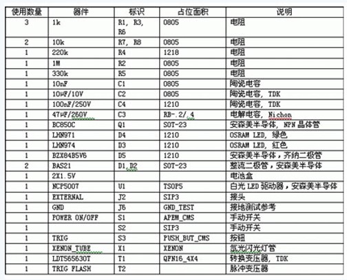
During Ton time, pin 12 of transformer T1 is low, so the battery voltage appears on pin 2 of the secondary side, which is the forward mode. The storage capacitor is charged by the current flowing through diode D1. After the start of the Toff cycle, the primary voltage is restored and the storage capacitor is charged by the current flowing through diode D2, which is the flyback mode of operation.
This concept is demonstrated by the demo board of Figure 3, which is powered by two standard alkaline AA dry batteries. The system is powered by switch S1, which is controlled by switch S2 connected to the start pin, and the third switch S3 is a button for manually triggering the flash.
The waveform in Figure 4 shows the voltage during the recharging of the storage capacitor. The signal corresponds to U1 pin 4 (upper curve), D1 pin 3 (middle curve) and D2 pin 3 (lower curve). When the U1 switch is activated, the forward mode occurs and the flyback cycle begins when the switch is turned off.
Ac To Dc Transformer,Ef High Frequency Transformer,Rm 10 Electric Transfomer,110 Volt Transformer
IHUA INDUSTRIES CO.,LTD. , https://www.ihua-sensor.com