The first chapter is the AM824-Core development kit . This article introduces the 1.5 MicroPort module and the 1.6 MiniPort module .
1.5 MicroPort Module Introduction
MicroPort is a standard micro-expansion interface that can be used to expand various peripheral modules and stack them for different applications. The peripheral modules that support the MicroPort interface are: SPI Flash module (MicroPort-Flash), EEPROM module (MicroPort-EEPROM). ) and RTC module (MicroPort-RTC).
> > > 1.5.1 SPI Flash Module
SPI Flash module (MicroPort - Flash), according to the MicroPort interface, the control pin is taken out to facilitate connection with the host supporting the MicroPort interface. See Figure 1.25(a) for details. MicroPort-Flash uses Wanghong's secure flash product MX25L1608D, which can be accessed via the SPI standard interface. Its capacity is 16Mb, typical rewritable 100,000 times, and data can be kept for 20 years. The function definition of the MicroPort interface (P1 port) in which the SPI Flash module (MicroPort-Flash) is plugged into the main controller is shown in Figure 1.25(b). The MCU is directly connected to the SPI Flash module (MicroPort - Flash) through the MicroPort interface to access the Flash. The pin function description is shown in Table 1.9.
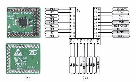
Figure 1.25 SPI Flash Module Physical Map and Interface Definition
Table 1.9 SPI Flash Module Function Pin Description

[1] There is no lead-out by default, and the corresponding 0-ohm resistor can be selected according to the actual situation;
[2] The default is not taken out. This function overlaps with the 5th bit function by default. If the 5th bit function conflicts with other modules, the nCS function can be switched to this pin through the 0Ω resistor.
The specific circuit of the SPI Flash module (MicroPort-Flash) is shown in Figure 1.26. The R3 and R4 resistors in the actual hardware are not soldered. The default nWP and HOLD are not taken out. If necessary, the test can be performed by soldering R3 and R4.
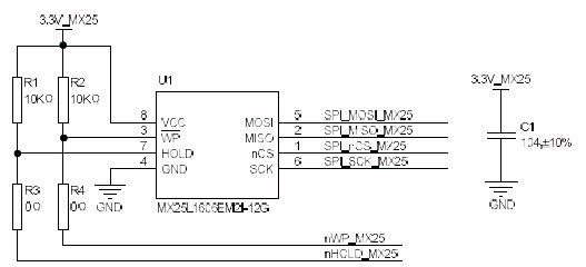
Figure 1.26 SPI Flash Module Circuit
> > > Â Â 1.5.2 EEPROM module
The EEPROM module (MicroPort-EEPROM), according to the MicroPort interface, pulls out the control pins for easy connection with the host that supports the MicroPort interface. See Figure 1.27(a) for details. The function definition of the MicroPort interface (P1 port) in which the EEPROM module (MicroPort-EEPROM) is inserted on the main controller is shown in Figure 1.27(b).

Figure 1.27 EEPROM module physical map and interface definition
The MCU is directly connected to the EEPROM module (MicroPort-EEPROM) through the MicroPort interface to access the EEPROM. The pin function description is shown in Table 1.10.
Table 1.10 EEPROM Module Function Pin Description

MicroPort – EEPROM uses Fudan Micro-semiconductor's FM24C02C with a capacity of 2048 bits (256 bytes), which can be accessed using the I2C interface. The default 7-bit slave address is 0x50, and the hardware circuit is shown in Figure 1.28.
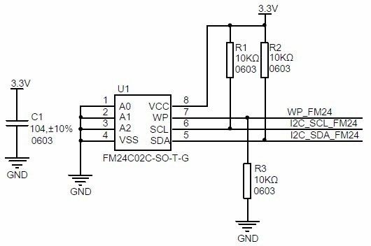
Figure 1.28 EEPROM Module Circuit
> > > Â Â 1.5.3 RTC Module
The RTC module (MicroPort-RTC) is based on NXP's PCF85063AT clock chip, which is a CMOS real-time clock and calendar. It is ideal for low-power applications. All addresses and data can be transmitted over the I2C bus. 400 kbit/s. The module pulls out the control pins according to the MicroPort interface, which is easy to connect with the main controller that supports the MicroPort interface. See Figure 1.29(a) for details. The definition of the MicroPort interface (P1 port) function of the clock module (MicroPort-RTC) plugged into the main controller is shown in Figure 1.29(b). The MCU is directly connected to the clock module (MicroPort-RTC) through the MicroPort interface to access the PCF85063. The pin function description is shown in Table 1.11.
Table 1.11 Clock Module Function Pin Description

Note: The default is not taken out, and the corresponding 0 ohm resistor can be selected according to the actual situation.
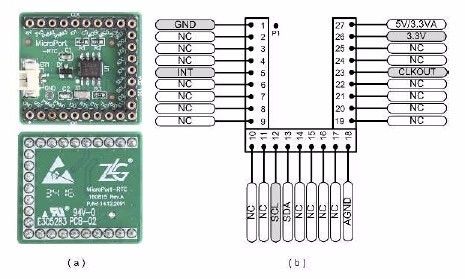
Figure 1.29 Clock module physical map and interface definition
The MCU uses the I2C interface to access the MicroPort-RTC. The default 7-bit slave address is 0x51. The hardware circuit is shown in Figure 1.30. In the actual hardware, the R1, R2 and R3 resistors are not soldered. The default CLKOUT and INT functions are not taken out. If necessary, the corresponding resistors can be tested. INT Two positions can be selectively welded according to the actual application. The two positions are designed to avoid conflicts between functions in the application and other modules, and provide as many options as possible.
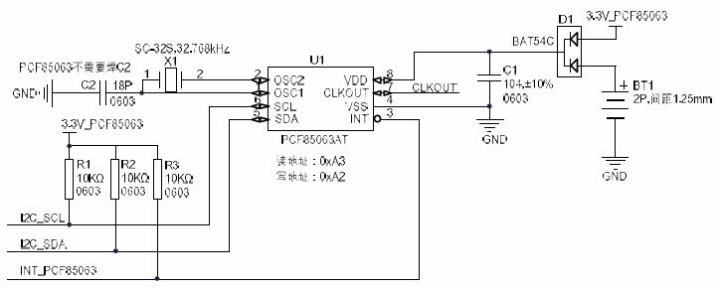
Figure 1.30 RTC Module Circuit
Note: The SDA, SCL and INT pins of the PCF85063/PCF8563 are open-drain structures. The actual application must be connected to a pull-up resistor.
The C2 in Figure 1.30 is not soldered by default. The PCF85063 has integrated load capacitors inside, and no external connection is required. This circuit is compatible with PCF8563. PCF8563 requires external capacitors at C2. D1 is a common cathode dual diode. The main function is to isolate the battery from the 3.3V power supply when the J1 interface is connected to the external battery. This prevents the battery from being wasted by 3.3V to other systems. The 3.3V system directly charges the battery (usually it is not rechargeable). battery).
> > > 1.5.4 USB module
The USB module (MicroPort-USB) is based on EXAR's XR21V1410IL16TR-F full-speed USB-UART converter chip. Its USB interface conforms to the USB2.0 specification and supports a data transfer rate of 12Mbps. The module pulls out the control pins according to the MicroPort interface, which is easy to connect with the main controller that supports the MicroPort interface. See Figure 1.31(a) for details. The function definition of the MicroPort interface (P1 port) in which the USB module (MicroPort-USB) is plugged into the main controller is shown in Figure 1.31(b).
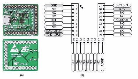
Figure 1.31 USB Module Physical Map and Interface Definition
The MCU is directly connected to the USB module (MicroPort-USB) through the MicroPort interface to control the USB module. The pin function description is shown in Table 1.12.
Table 1.12 USB Module Function Pin Description

XR21V1410IL16TR-F Full-speed USB-UART conversion chip, its USB interface conforms to USB2.0 specification and supports data transmission rate of 12Mbps. The hardware circuit is shown in Figure 1.32. The module inputs data through the MicroUSB socket, converts it to serial port data, and then communicates with the master MCU to realize the USB to serial port function. The module comes with a 5V to 3.3V power chip U3, no additional power supply to the backplane, and its output current can reach 300mA, which meets the working requirements of XR21V1410IL16TR-F. The ESD protection diode U2 provides reliable ESD protection for the USB interface circuitry.
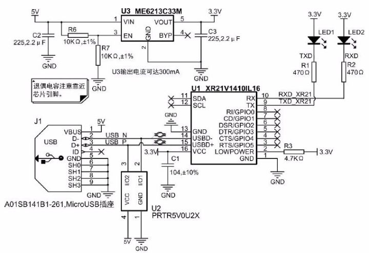
Figure 1.32 USB Module Circuit
> > > Â Â 1.5.5 RX8025T Module
The RX8025T module (MicroPort-RX8025T) is based on EPSON's I2C bus real-time clock chip RX-8025T. This model has a high stability 32.768KHz DTCXO (Digital Temperature Compensated Crystal Oscillator), in addition to the calendar function and clock counting function. The chip also offers a wealth of other features such as an alarm clock, a fixed-cycle timer, a time-update interrupt, and a clock output. The module pulls out the control pins according to the MicroPort interface, which is easy to connect with the host that supports the MicroPort interface. See Figure 1.33(a). The function definition of the MicroPort interface (P1 port) of the RX8025T module (MicroPort - RX8025T) plugged into the main controller is shown in Figure 1.33(b). The MCU is directly connected to the RX8025T module (MicroPort-RX8025T) through the MicroPort interface to realize the control of the RX8025T module. The pin function description is shown in Table 1.13.
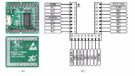
Figure 1.33 RX8025T module physical map and interface definition
Table 1.13 RX8025T Module Function Pin Description

The MCU uses the I2C interface to access the MicroPort - RX8025T. The read address is 0x65h and the write address is 0x64h. The hardware circuit is shown in Figure 1.34. The circuit design is compatible with the RX8025SA, but the RX-8025T has only one interrupt output function. The MicroPort interface P1 Pin5 leads. The RX-8025T chip has a high-precision 32.768kHz crystal that enables high-precision real-time timing without an external crystal. The interrupt output pin is connected to the system power supply by a pull-up resistor to ensure that its pin is at a stable level when the interrupt output function is not used. D1 is a common cathode dual diode. The main function is to isolate the battery from the 3.3V power supply when the P1 interface is connected to the external battery. This prevents the battery from being powered by 3.3V to other systems. The 3.3V system directly charges the battery (usually non-rechargeable here) battery).
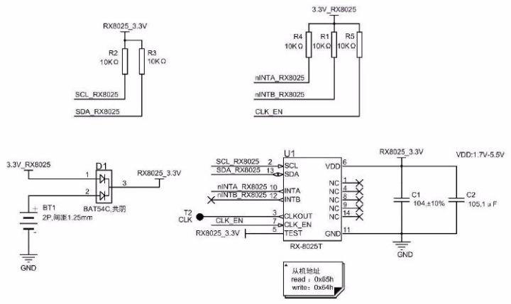
Figure 1.34 RX8025T Module Circuit
> > > 1.5.6 DS1302 Module
The DS1302 module (MicroPort-DS1302) is based on DALLAS's high-performance, low-power, real-time clock chip with RAM, which can time the year, month, day, week, hour, minute and second, with leap year compensation. The working voltage is 2.0V~5.5V, and it has a fine current charging capability. The module pulls out the control pins according to the MicroPort interface, which is easy to connect with the host that supports the MicroPort interface. See Figure 1.35(a). The function definition of the MicroPort interface (P1 port) in which the DS1302 module (MicroPort-DS1302) is plugged into the main controller is shown in Figure 1.35(b).
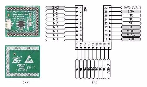
Figure 1.35 DS1302 module physical map and interface definition
The MCU is directly connected to the DS1302 module (MicroPort-DS1302) through the MicroPort interface to control the DS1302 module. The pin function description is shown in Table 1.14.
Table 1.14 DS1302 Module Function Pin Description

The DS1302 uses a three-wire interface for synchronous communication with the MCU. An externally connected 32.768kHz crystal provides an accurate clock source. The accuracy of the clock depends on the accuracy of the crystal and the pin load capacitance of the crystal. The chip has a main power/backup power dual supply pin, where the main power supply VCC2 is connected to the system power supply 3.3V_DS1302, the backup power supply VCC1 is connected to the battery, and the DS1302 is powered by the larger of VCC1 or VCC2. When VCC2 is greater than VCC1+0.2V, VCC2 supplies power to the chip. When VCC2 is less than VCC1, the chip is powered by VCC1, so the clock can be kept running continuously when the main power is off. The detailed hardware circuit is shown in Figure 1.36.

Figure 1.36 DS1302 Module Circuit
> > > Â Â 1.5.7 Analog Module
The Analog Module (MicroPort-Analog) is a low-power, high-performance analog signal acquisition and output module based on the 3Peak LMV358A op amp chip. The function definition of the MicroPort interface (P1 port) in which the Analog module is plugged into the main controller is shown in Figure 1.37(b).
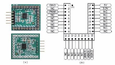
Figure 1.37 Analog Module Physical Map and Interface Definition
The MCU is directly connected to the Analog module (MicroPort-Analog) through the MicroPort interface to connect to the AD acquisition channel and control the DA output channel. The pin function description is shown in Table 1.15.
Table 1.15 Analog Module Function Pin Description
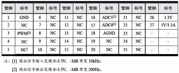
MicroPort - Analog consists of two 3rd-order low-pass filters for ADC drive and anti-aliasing filtering, and a 6th-order low-pass filter for PWM DACs. The module can be used together with the MCU to better utilize the on-chip ADC performance of the MCU. When the ADC function is used, the input pin of the filter is directly connected to the signal source to be acquired, and the signal input function of the high input impedance is realized. The input range of the signal is 0~3.3V, the hardware circuit is shown in Figure 1.38.
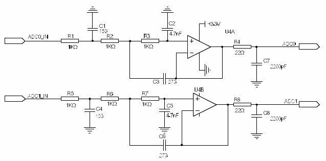
Figure 1.38 ADC Driver Circuit
When the PWM DAC function is used, the output pin of the filter is processed by the filter to obtain an analog voltage value proportional to the duty ratio, which can realize the DAC function, has low output impedance, and the signal output range is 0~3.3V. The hardware circuit is shown in Figure 1.39.
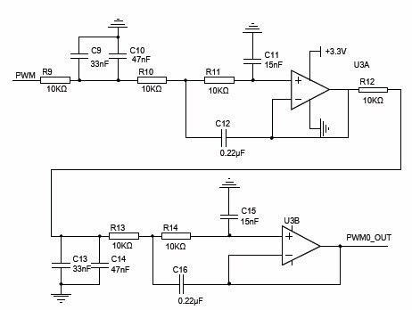
Figure 1.39 DAC Filter Circuit
1.6 MiniPort Module Description
> > > Â Â 1.6.1 LED module
The LED module (MiniPort-LED) integrates 8 LEDs, and the control pins are led out according to the MiniPort interface, which is easy to connect with the host supporting the MiniPort interface. It can be controlled by 8 I/Os. The definition of the function of the MiniPort interface (J4B port) of the LED module is shown in Figure 1.40. The function of the MCU through the MiniPort interface to drive the LED module (MiniPort-LED) is described in Table 1.16. .
Table 1.16 LED Module Pin Description
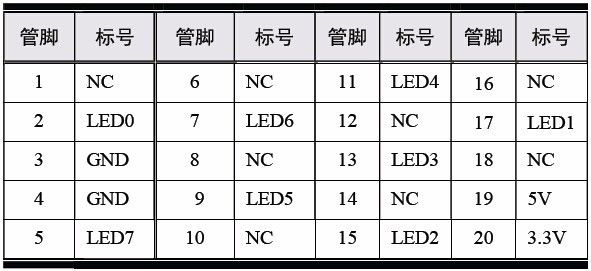
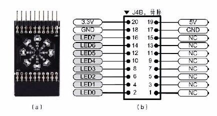
Figure 1.40 LED module physical and interface definition map
The LED module (MiniPort - LED) circuit is shown in Figure 1.4.1, where the LED is active low (low level). The LED module (MiniPort - LED) is controlled by connecting the MiniPort B to the MiniPort A.
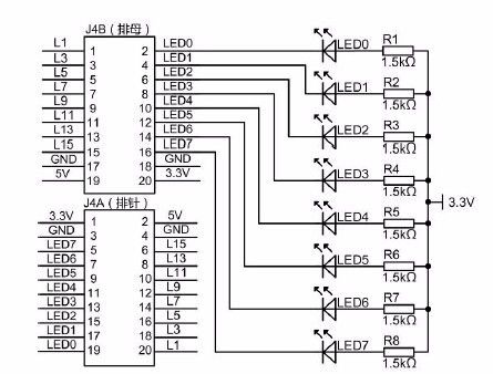
Figure 1.41 LED Module Circuit
The LED module is connected to the main controller backplane through the MiniPort B, and the remaining unused I/Os are led out through the MiniPort A (bent needle) for horizontal stacking of the modules. L1~L15 means that the corresponding interfaces that are not used by the A/B interface are connected to facilitate stacking and expansion.
> > > 1.6.2 Digital Tube Module
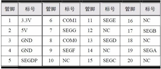
The digital tube module (MiniPort-View) integrates two eight-segment digital tubes, and the control pins are led out according to the MiniPort interface, which is convenient for connecting to the host supporting the MiniPort interface. Through COM0, COM1 control digital tube bit selection, seg A~segDP connected to the SEG end of the digital tube, the digital tube module corresponding to the main controller MiniPort interface (J4 port) function definition is shown in Figure 1.42. The function description of the MCU through the MiniPort interface to drive the digital tube module (MiniPort-View) pin is shown in Table 1.17.
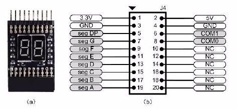
Figure 1.42 Digital tube module physical and interface definition map
Table 1.17 Digital Tube Module Pin Description
The digital tube module (MiniPort - View) consists of two common digital tubes LN3461BS. The specific circuit is shown in Figure 1.43. The seg A~seg DP 8 ports are used as the interface for driving the digital pipe segment. The 470 ohm current limiting resistor is connected to the segment selection terminals (a, b, c, d, e, f, g, dp) of the digital tube. COM0 and COM1 are used as bit selection control bits, connected to the base of the PNP type transistor through a 5.1K resistor. The emitter of the triode is connected to the 3.3V power supply, and the collector is connected to the bit selection segment of the digital tube. Since the eight segments of the digital tube need to be powered by the COM terminal, only the MCU's I/O current driving capability is limited. For this reason, a triode is added to the design to increase the COM terminal driving current.
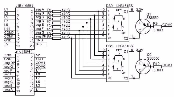
Figure 1.43 Digital tube module circuit diagram
The digital tube module is connected to the host through the MiniPort B, and the other unused I/Os are taken out through the MiniPortA (bent needle) to realize horizontal stacking of the modules. L1~L11 means that the corresponding interfaces that are not used by the A/B interface are connected to facilitate stacking and expansion.
> > > Â Â 1.6.3 Button Module
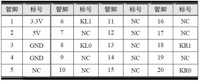
The button module (MiniPort - Key) integrates 4 buttons, and the control pins are led out according to the MiniPort interface, which is convenient for connection with the main controller supporting the MiniPort interface. The function definition of the button module corresponding to the main controller MiniPort interface (J4 port) is shown in Figure 1.44. The function description of the MCU through the MiniPort interface control button module (MiniPort-Key) pin is shown in Table 1.18.
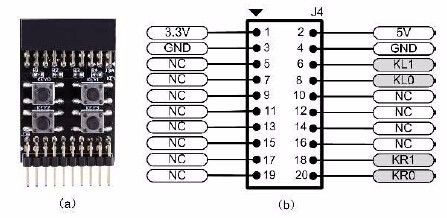
Figure 1.44 Button module physical and interface definition map
Table 1.18 Button Module Pin Description
The circuit of the button module (MiniPort-Key) is shown in Figure 1.45. It is arranged by matrix keyboard. KR0 and KR1 are row lines, KL0 and KL1 are column lines, and the column lines are shared with the digital tube COM segment. When the dynamic display and dynamic scan of the button are realized, the operation of COM0, COM1, KL0, and KL1 is the same. The digital tube driver sequentially lowers COM0 and COM1 to select the digital tube to be lit. The button scan driver is sequentially turned down. KL0 and KL1, through the values ​​of KR0 and KR1 to judge the state of the button, so KL0, KL1 and COM0, COM1 can be reused according to the working characteristics of the two), when the module is shared with the digital tube module, Reduce I/O usage.
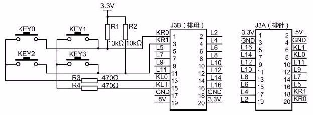
Figure 1.45 Button Module Circuit
In Figure 1.45, R3 and R4 only play the role of protection isolation. If there is no R3 and R4, and KL0 and KL1 are directly connected to the corresponding column line of the matrix keyboard, there will be such a potential problem in the keyboard circuit: if KL0 is set to 0 (Low level), KL1 is set to 1 (high level). At this time, if KEY0 and KEY1 (KEY2 and KEY3) are pressed at the same time, a short circuit is formed between two I/Os of KL0 and KL1.
The button module is connected to the host through the MiniPort B, and the other unused I/Os are taken out through the MiniPort A (bent needle) to realize horizontal stacking of the modules. L1~L16 means that the corresponding interfaces that are not used by the A/B interface are connected to facilitate stacking and expansion.
> > > Â Â 1.6.4 595 module
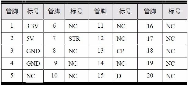
The 595 module (MiniPort - 595) is mainly used for I/O expansion. The module uses the 74HC595 chip to expand 8-way I/O by serial transfer. The 595 module can directly drive the LED module or drive the digital tube module with the COM0 and COM1 pins. The 74HC595 chip uses three control pins, which are the CP clock signal pin, the D data pin, and the STR latch signal pin. The function definition of the 595 module corresponding to the main controller MiniPort interface (J4 port) is shown in Figure 1.46(b). The output signal of the 595 module is taken out through the MiniPort A (bend pin) (MiniPort-595 J2A port). The pin function definition is shown in Figure 1.46(c). The MCU controls the 595 module (MiniPort - 595) pin function through the MiniPort interface. Table 1.19.

Figure 1.46 595 module physical and control interface definition map
Table 1.19 595 Module Control Pin Description
The circuit of the 595 module is shown in Figure 1.47, the MiniPort B is the input interface of the 595 module, and the MiniPort A is the output interface of the 595 module. It is connected to the LED, digital tube and other modules through this interface.
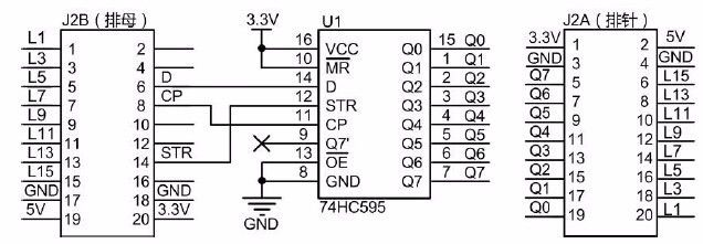
Figure 1.47 595 module circuit diagram
Since the 595 module is mainly used for peripheral expansion, the pins on both ends of MiniPort A and MiniPort B are not identical. L1~L15 means that the corresponding interfaces of the 595 module A/B interface are not connected, which is convenient for stack expansion.
> > > Â Â 1.6.5 ZLG72128 Module
The MiniPort-ZLG72128 module can manage 2 common buttons, 2 function buttons and 2 common digital tubes. The unit is connected to the AMetal824 platform via a 10×2 pin interface and is operated and demonstrated via the I2C interface of the AMetal824. ZLG72128 module's main control chip is ZLG72128, which is a digital tube display driver and keyboard scanning management chip designed by Guangzhou Zhouligong SCM Technology Co., Ltd. Its main features:
Direct drive 12-bit cascode (less than 1 inch) or 96 independent LEDs;
Ability to manage up to 32 buttons to automatically eliminate jitter, 8 of which can be used as function keys;
The power circuit can easily drive large digital tubes of more than 1 inch;
Powerful functions such as bit flicker, bit blanking, segment lighting, segment extinction, function keys, and combo key counting;
Provides 10 types and 21 letters of decoding display function, or directly writes display data to the display buffer;
I2C serial bus interface is used with the microcontroller, only two signal lines are needed to save I/O resources;
Operating voltage range: 3.0 ~ 5.5V;
Operating temperature range: -40 to +85 ° C;
Package: Standard TSSOP28.
The ZLG72128 module is pulled out via MiniPort A (bend pin) (MiniPort-595 J2A port). The pin function definition is shown in Figure 1.48. The I2C interface of the ZLG72128 requires only two signal lines, SDA and SCL, and its address: 1100000 read/write (1/0). The corresponding circuit schematic is shown in Figure 1.49.
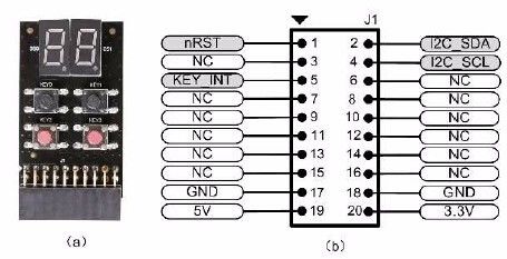
Figure 1.48 MiniPort-ZLG72128 Physical and Interface
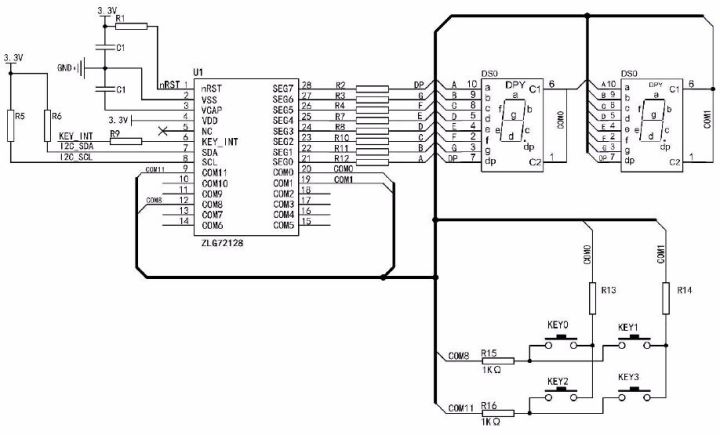
Figure 1.49 MiniPort-ZLG72128 Module Schematic
We are a professional screen protector manufacturer, providing one-stop product production solutions, providing exclusive OEM and ODM services. A wide range of products, including HD Clear Screen Protectors, Self-repair Screen Protectors, Anti-microbial Screen Protectors, Matte Screen Protectors, Privacy Screen Protectors and other series.
We are committed to the development, production and sales of hydrogel screen protectors. We strictly control the screen protector production process to ensure that each product meets industry standards. If you want to know more products, please click the product details to view.
Whether you are a group or an individual, we will do our best to provide you with the best service and the most accurate and comprehensive product information!
Universal Screen Protector, TPU Screen Protector, Hydrogel Protective Film, Mobile Phone Screen Protector, Hydrogel Screen Protector, TPU Protective Film
Shenzhen Jianjiantong Technology Co., Ltd. , https://www.jjthydrogelprotector.com