Practice has shown that in many applications, properly filtered switching converters can replace linear regulators to produce low noise power supplies. Even in demanding applications where very low noise power supplies are required, switching circuits may be present somewhere in the upstream power tree. Therefore, it is necessary to design a multi-stage filter that is optimized and damped to eliminate the output noise of the switching power converter. In addition, it is important to understand how the filter design affects the compensation of the switching power converter.
Recently, switching power supplies have been used in almost all electronic devices. They are extremely valuable due to their small size, low cost and high efficiency. However, their biggest drawback is that high switching transients result in high output noise. This shortcoming makes them unusable in high-performance analog circuits that are powered by linear regulators.
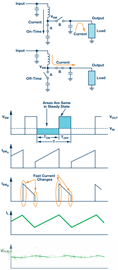
The example circuit in this article will use a boost converter, but the results can be directly applied to any DC-DC converter. Figure 1 shows the basic waveform of the boost converter in constant current mode (CCM).

Figure 1. Basic voltage and current waveforms of the boost converter
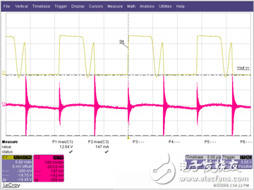
The output filter is important for the boost topology or any other topology with a discontinuous current mode because it has a fast rise and fall time in switch B. This can result in parasitic inductance in the excitation switch, layout, and output capacitors. As a result, in actual use, the output waveform looks more like Figure 2 rather than Figure 1, even if the layout is good and ceramic output capacitors are used.

Figure 2. Typical measurement waveform of a boost converter in DCM
The switching ripple (switching frequency) due to the change in capacitance charge is very small compared to the undamped ringing of the output switch, hereinafter referred to as output noise. In general, this output noise ranges from 10 MHz to over 100 MHz, well beyond the self-resonant frequency of most ceramic output capacitors. Therefore, adding additional capacitance has little effect on noise attenuation.
There are also many types of filters suitable for filtering this output. This article will explain each filter and give each step of the design. The formulas in the paper are not rigorous, and some reasonable assumptions have been made to simplify these formulas to some extent. Some iterations are still needed because each component affects the values ​​of other components. The ADIsimPower design tool avoids this problem by using a linearization formula of component values ​​(such as cost or size) to optimize the components before actually selecting them, then selecting the actual components from a database of thousands of devices and optimizing their output. . But at the beginning of the design, this level of complexity is not necessary. With the calculation formula provided, using a SIMPLIS simulator – such as the free ADIsimPETM – or spending some time on the lab bench, you can get a satisfactory design with minimal effort.
Before you start designing the filter, consider what a single-stage filter RC or LC filter can do. A secondary filter is typically used to properly reject ripple to a few hundred μV pp and to suppress switching noise below 1 mV pp. The buck converter is less noisy because the power supply inductance provides good filtering capability. These limitations are due to the fact that once the ripple is reduced to the μV level, the noise coupling between the component parasitics and the filter stage begins to become a limiting factor. If a less noisy power supply is used, a three-stage filter is required. However, the reference voltage source for a switching power supply is generally not the lowest noise component and is often affected by jitter noise. These all result in low frequency noise (1 Hz to 100 kHz) and are usually not easily filtered out. Therefore, for very low noise power supplies, it may be more appropriate to use a single secondary filter and then add an LDO at the output.
Before describing the design steps of each type of filter in more detail, some of the values ​​of the various types of filters used in the design steps are defined as follows:
Enter the peak-to-peak current approximation of the output filter. For the convenience of calculation, it is assumed to be a sinusoidal signal. The value depends on the topology. For a buck converter, it is the peak-to-peak current in the inductor. For a boost converter, it is the peak current in switch B (usually a diode).
Approximate output voltage ripple at the converter switching frequency.
The ESR of the selected output capacitor.
Converter switching frequency.
In the calculation of the output capacitance, it is assumed that all flow into it.
Insulation Paper Dmd,Insulfrax Paper,Silver Paper Insulation,Battery Insulation Paper
Longkou Libo Insulating Material Co.,Ltd. , https://www.liboinsulation.com