This article discusses how a high-performance clock generator works with one or more integrated transceivers to simplify the overall design, reduce complexity and cost, and achieve excellent system reception and transmission performance. Even if the base station loses the timing reference signal for a long time, all other base stations in the network can still maintain synchronization. For telecom base stations, system architects need to spend considerable effort and time to design high-performance clocks and sine wave oscillation circuits. Although a single-chip transceiver integrates many such signal generators, it still requires a reference clock. The base stations in a network are generally synchronized with each other, so the reference clock must keep the timing consistent with a network-wide timing signal.
One of the most frequently mentioned base station parameters for base station clock architecture is its carrier (or local oscillator) frequency. The frequency synthesizer that generates the local oscillator is an important part of the base station, but as all system designers know, the local oscillator is just one of the multiple internal frequencies required by the base station. For the transceiver alone, in addition to providing the local oscillator (LO) of the carrier frequency to the mixer stage, the data converter requires a sampling clock, the digital filter requires a clock, and the I / O bus usually requires a data clock.
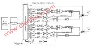
Using integrated transceivers, system architects can save a lot of design time and cost, as shown by the dotted box in Figure 1. In addition to the receiver and transmitter circuits, the single-chip transceiver also integrates a phase-locked loop (PLL) to generate the clock and sinusoidal signals required by various signal processing modules. However, even highly integrated transceivers also require a reference clock input.
Single-chip 2 × 2 multiple-input / multiple-output (MIMO) transceivers such as the AD9356 and AD9357 from Analog Devices offer two different reference clock options. One is to use an external crystal with the on-chip digital control adjustment circuit (DCXO), and the other is to provide an external clock for the device. AD9356 / 7 accepts the reference clock frequency in the range of 32-48MHz.
User stations such as user equipment (CPE) use information sent by the base station to synchronize with the wireless network. The CPE equipment will fine-tune its local oscillator frequency, and it will also keep time synchronized with the base station's main clock. Therefore, the above external crystal plus DXCO option is a low-cost, high-performance solution for this application.
The base station will have other requirements. For example, operators often require that the frames and symbol boundaries of all sites in a particular network be consistent in timing. Since the base station is responsible for providing timing information to its related user stations, this requirement means that all base stations in the network must be locked to an external timing reference. There are generally two ways for system architects to synchronize base stations. One method is to use the 1pps (pulse / second) output provided by the GPS receiver, and the other method uses the network timing protocol specified by the IEEE 1588 standard. In any case, the transceiver reference clock input shown in Figure 1 is synchronized with the timing reference (for example, a 1pps GPS clock).
Base station reference clock design considerations are shown in Figure 1. The integrated transceiver uses the reference clock as the input to the PLL. If it is an RF PLL, the base station will multiply the reference clock up to the LO frequency. This multiplication factor can be 8 or greater. Therefore, for the transceiver to achieve high performance, the phase noise of the reference clock must be very low.

Figure 1 2x2 MIMO base station transceiver architecture
The reference clock must also be synchronized with the external timing reference, which is 1pps for GPS.
An important result of synchronization is the concept of "holding". If the timing reference is lost (for example, the building blocks the GPS satellite signal at certain times of the day), the reference clock must remain in the same state as the timing reference. Standards such as ANSI / T1.101-19873 divide maintenance requirements into multiple levels, each of which specifies different maximum deviations allowed within a specific time. Stratum 3E is an additional layer defined by Bellcore GR-1244-CORE4, which requires that the clock source's offset within 24 hours must not exceed one hundredth of a billion.
As described in the N × N MIMO system section below, if a base station uses two or more transceivers in a multiple input multiple output architecture, the base station must synchronize all transceivers with the same timing reference. To reduce the number of devices and cost, the reference clock should be able to provide multiple identical outputs, each of which can drive different transceiver modules.
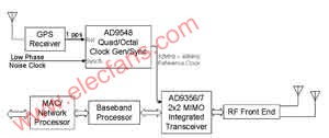
Case study: providing an external clock This case study uses the AD9356 / 7 2 × 2 MIMO integrated transceiver as part of the base station system. As mentioned earlier, the AD9356 / 7 requires a reference clock frequency of 32 to 48 MHz. To synchronize this clock with the timing reference, a flexible PLL with excellent phase noise performance is required. Like the AD9548 4/8 channel input network clock generator / synchronizer from Analog Devices, this requirement is fully met. The timing reference output is connected to one reference input of the AD9548, and a low phase noise clock is connected to the system clock input. The output is set to the 32-48MHz reference clock required by the AD9356 / 7. Figure 2 shows a block diagram of a GPS synchronization system.

Figure 2 Base station architecture using GPS reference
Some network clock generators can support a very wide input frequency range, thereby providing various timing references and low phase noise clocks. Choosing the input frequency wisely can simplify the design, reduce costs, achieve the best transmission and reception performance, and meet the maintenance performance requirements.
The AD9548 uses a digital phase-locked loop (DPLL) to lock the output clock to the timing reference instead of the analog PLL. This technique allows the system to achieve excellent retention performance, limited only by the timing drift of the system clock source. In addition, the factor that determines the phase noise performance of the AD9548 output clock is the phase noise of the system clock, not the timing reference, so the device can accept a high-noise timing reference without passing this noise to its output.
Achieve the highest reference clock performance The network clock generator supports a wide range of input and output frequencies, thus providing system architects with many options for optimizing output clock performance.
For example, high-stability clock sources with frequencies of 25 MHz and below are relatively richer and cheaper than higher-frequency clock sources. If the system clock (sysclk) input shown in Figure 2 is less than 50MHz, the frequency multiplier in the AD9548 can be used to double the system clock, and the added phase noise is extremely small. Then using this higher frequency, the system clock PLL can raise the clock to about 1 GHz.
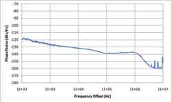
The designer must also choose the DPLL output frequency and the resulting postscaler ratio. The higher the DPLL output frequency, the faster the slew rate, which generally helps reduce phase noise, but may also cause spurs to fold back into the spectrum. For the AD9356 / 7 reference clock, an effective compromise is to set the DPLL output frequency to 240MHz and set the post-division ratio to 6 to obtain a final output frequency of 40MHz. Figure 3 shows the phase noise of the AD9548 at these settings.

Figure 3 Relationship between phase noise and frequency of AD9548 from Analog Devices
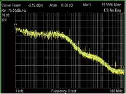
Figure 4 shows the integrated phase noise at the output of the AD9356 when using the AD9548 to provide a reference clock and transmitting at 2500MHz. The AD9548 evaluation board can utilize its own on-chip system clock XO (factory configuration) or external clock. Figures 3 and 4 show the AD9548 using a 12.8MHz constant temperature control crystal (OCXO) as its system clock input. In this test, the AD9548 was not synchronized with the timing reference.

Figure 4 Analog Devices AD9356 integrated phase noise, 2500MHz carrier
In this configuration, when using the WiMAX 802.16e 64-QAM waveform, the typical EVM value at the output of the AD9354 is better than -38dB.
As mentioned earlier, to ensure that the final EVM of the transceiver is as low as possible, the system clock source of the network clock generator must have low phase noise. In addition, the system clock source must have excellent short-term stability, especially when the 1pps signal is used as a network timing reference. To synchronize with the GPS timing reference, the network clock generator must use a very narrow PLL bandwidth. Therefore, the system clock source must have very low jitter to keep the network clock generator PLL locked. High-performance clock sources such as OCXO meet these requirements and are therefore commonly used by base stations.
NxN MIMO system
NxN MIMO systems require multiple transceivers, and each transceiver requires the same version of an external reference clock. The network clock generator can provide multiple identical outputs, which can be routed to each transceiver separately, thereby eliminating clock buffers and clock distribution devices.
The AD9548 can provide up to 4 differential LVDS / LVPECL outputs or 8 single-ended CMOS outputs. The solid line box and signal in FIG. 5 represent a 4 × 4 MIMO system with a common phase-locked reference clock, and the dashed line and dashed box indicate that the system is extended to a 6 × 6 MIMO architecture.

Figure 5 NxN MIMO base station architecture using GPS timing reference
The sampled data is transmitted between the AD9356 / 7 and BBP through the JESD-207 compatible parallel port interface, and the AD9356 / 7 generates the parallel port data clock. In 4 × 4 and higher order systems, BBP can simultaneously send pulses to each transceiver of the AD9356 / 7, thereby forcing the data clocks of all transceivers to be synchronized. This can ensure that the sampling data sent and received by each transceiver keeps the same timing.
Conclusion High-performance clock generators can be synchronized with external timing references and work with one or more integrated transceivers, thereby simplifying the overall design of telecommunications base stations and reducing complexity and cost. The design can be easily extended to NxN MIMO base station architecture. These devices integrate most of the clock and sine wave generators while still achieving excellent system reception and transmission performance. Even if the timing reference signal is temporarily lost, the base stations in the network can synchronize with each other.
PV pumping system is the use of solar modules to solar energy directly into electrical energy, drive motor driven pump device. Mainly divided into submersible pumps photovoltaic pumping and ground pumping photovoltaic pumping (suction stroke, different installation methods); PV pumping system: no fuel consumption, no power grid, almost no need for operation and maintenance, long service life, low average cost, especially for water and electricity shortage areas. Do not need batteries, solar modules directly driven by the pump work.
Solar Pump System,Solar Water Management System, Water Transfer Pump,Pumping Stations,DC Pump
Wuxi Sunket New Energy Technology Co.,Ltd , https://www.sunketsolar.com