Review the history of storage. 3D Xpoint is one of the most groundbreaking storage technologies since the introduction of NAND Flash. With the following four advantages, 3D Xpoint is seen as a disruptor in the storage industry:
(1) 1000 times faster than NAND Flash;
(2) The cost is only half of DRAM;
(3) The service life is 1000 times that of NAND;
(4) The density is 10 times that of traditional storage;
Thanks to these advantages, 3D Xpoint can be widely used in games, media production, genome sequencing, financial services trading and individualized treatment. These are just some application examples for 3D Xpoint. But from the above introduction, we can see that the future application of 3D Xpoint has great potential.
Some problems with the current memory
The performance of the memory is the current short board on the PC device. This point is reflected in the fact that many users have changed from HDD to SSD, and it feels like "changing a computer". The current transmission speed of HDD is often within 200MB/s, the seek time is about 10ms; the SSD transmission speed is hundreds of MB/s to several GB/s, and the seek time is about 0.1ms; the faster memory bandwidth is Dozens of GB/s, delay time as low as ns. There are also higher speed caches, registers and other devices.
DRAM: Volatility is difficult to solveAside from the cache and registers that are closely related to the processor, let's look at the two levels of memory and external storage. The memory we currently use is mainly DRAM. The core problem of DRAM is volatility, and other aspects of performance are excellent - for example, DRAM latency is very low (nanosecond level), bandwidth is sufficient; life expectancy is due to the principle, DRAM life is very long. However, DRAM storage requires constant power supply, and lost data will lose stored data. From the invention of DRAM to the present, DRAM is only constantly adjusted on pre-fetch values ​​and buses, and the core storage architecture has not changed much.
NAND: life expectancy and delay are not satisfactoryLet's look at NAND flash memory that is currently widely used in storage devices. NAND flash memory is divided into various branching particles such as SLC, MLC, and TLC. In terms of lifetime, NAND has an average number of read and write times, and even the best performing SLC NAND particles have a much smaller lifetime than DRAM. Although it is possible to ensure that NAND does not “drop the chain†and cause data loss by setting the buffer space, balancing the wear algorithm, and setting the life warning in advance, the lifetime is still an unavoidable problem in the use of NAND.
In addition, subject to the storage principle, NAND latency is high, especially when there is charging time when writing, how can it not be fast, and can only be used as an external storage device. But today, due to the existence of lower performance HDD mechanical hard drives, NAND particle-based SSDs still give users a huge performance boost.
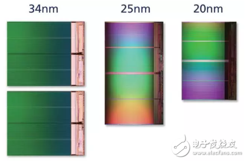
â–² As the process increases, the capacity of NAND is rapidly increasing, but there are no revolutionary changes in life and delay.
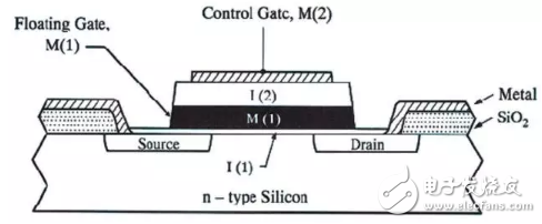
â–² NAND working principle diagram, insulated floating gate is the core of its stored data.
Performance Divide: Problems with PC ArchitectureThe so-called performance gap is that there is a large performance gap between the upper and lower systems, making it difficult for the design of the level cache to show the best effect. On NAND and DRAM, this gap is compared between DRAM and HDD. The performance gap has narrowed slightly, but the changes in nature are not obvious. For example, the current fastest speed of NAND devices is almost 2GB/s to 3GB/s, and the memory bandwidth of the processor has exceeded 50GB/s. The difference between the two is an order of magnitude. In terms of latency, DRAM is only a dozen nanoseconds, which is many orders of magnitude faster than NAND's about one hundred microseconds.
In fact, the performance gap between memory and external storage is too large, which has become a bottleneck that affects the user experience. So research institutions have been proposing many solutions to try to solve this gap, such as phase change memory, track memory, new high-speed magnetic storage devices. But these technologies are not hidden in the lab, they have just been made public on the PPT. Last year, Intel and Micron, one of the leaders in the storage industry, finally pushed one of the new storage technologies to the forefront. This technology has both high performance and non-volatile features. Protagonist: 3D XPoint!
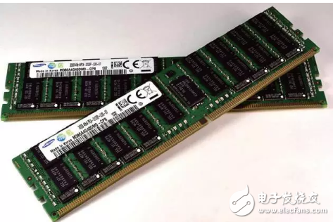
â–² The basic technical structure of memory has not changed revolutionually for a long time. The fastest DDR4 memory available today can only act as a scratchpad.
The principle of 3D XPointAt present, Intel and Micron are not talking about the physical characteristics of 3D XPoint applications, and the information is scarce. Some unnamed introductions show that the physical value of the tagged data state used by 3D XPoint is not the voltage or current used in the industry, nor is it the magnetic pole currently in the laboratory, but the resistance.
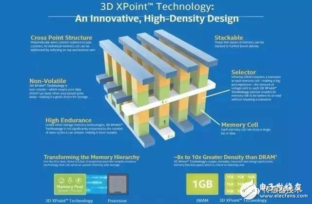
The working principle of 3D XPoint is fundamentally different from NAND. NAND captures different numbers of electrons through an insulated floating gate to define bit values, while 3D XPoint is a resistance-based storage technology that differentiates between 0 and 1 by changing the cell resistance level.
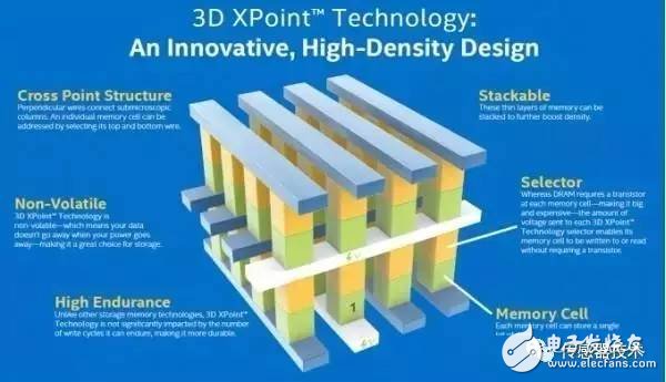
The structure of 3D XPoint is very simple. It consists of a selector and a memory unit, which exist between the word line and the bit line (so they are named with 'intersection'). Providing a specific voltage between the word line and the bit line activates a single selector and causes the memory cell to be written (ie, a large number of attribute changes in the memory cell material) or read (allowing to check whether the memory cell is in a low or high resistance state) ).
Assume that the write operation requires a higher voltage than the read, because if the actual situation is reversed, then the 3D XPoint will face the risk of triggering a large amount of material change (ie, write operation) when reading the memory cell.
Intel and Micron did not disclose the specific voltage value of internal read/write, but according to the message, the voltage should be lower than NAND - the latter needs to use about 20 volts to write/erase to create enough Electron tunneling through the electric field of the insulator. This lower voltage requirement naturally allows 3D XPoint to have lower operating power than DRAM and NAND.
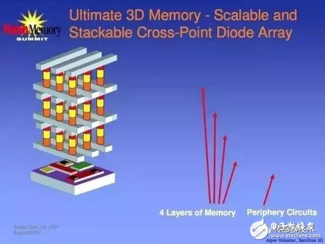
As the name suggests, 3D XPoint memory cells can be stacked in 3D to further increase storage density. The first generation of grain samples is currently using a two-layer design. The double layer sounds a bit chilly, especially considering that the current 3D NAND chip already has 32 layers and gradually begins to enter the 48th floor. However, the construction of 3D XPoint is completely different, and it is obviously not scientific to directly compare the layers.
In the manufacturing process, 3D NAND is first added with a deposited conductive layer, and then an insulating material is added over each layer. Only after the deposition of all the layers is completed, the entire "cell tower" can be defined by photolithography, and then the via material is filled in the high aspect ratio etching holes to realize mutual communication between the memory cells in the respective layers.
In contrast, each layer of 3D XPoint requires lithography and etching (ie, repeating the same process over each layer), followed by deposition of the next layer. This approach sacrifices some of the economic advantages of 3D NAND (ie, fewer lithography steps), but 3D XPoint brings a much higher storage density than pure lithography.
Intel and Micron pointed out that future process size scaling will occur in both lithography and layer 3D stacking. The horizontal and vertical scale tunability will be key to ensure that it will remain more malleable in the future, as traditional multi-mode immersion lithography based on argon fluoride has lost economic advantages at the 10 nm level. No clear succession techniques have yet to emerge.
The current industry is generally pinning its hopes on EUV, while Intel and Micron have confirmed that 3D XPoint will (unsurprisingly) be compatible with EUV lithography, and the size of the memory cell can be reduced to a single digit nanometer level - and will not It has a significant impact on the use of help/reliability (in fact, as physical dimensions decline, it improves in some ways).
However, in the next few years, I am afraid that it is still impossible to use EUV to achieve mass production. The main focus of the first EUV production will also be on the logic level, in part because the cost of equipment is too high, and on the other hand, because logic cannot bloom vertically like memory, it may cause heat dissipation.
Theoretically speaking, 3D XPoint also supports multi-level cell design, but Intel and Micron are not currently planning to pursue this route. Although it is not too difficult to achieve multiple resistance levels in the laboratory, the actual difficulty is much higher than the tens of thousands of wafers guaranteed to ensure that each die has the necessary characteristics to achieve double Layer unit operation.
In contrast, this idea is very similar to the fact that the 2-bit mechanism per unit just appeared in the NAND field 20 years ago, so Intel and Micron will temporarily focus on lithography and 3D scaling to improve Storage density and cost effectiveness. However, I believe that in the future, multi-level cell design will gradually appear in 3D XPoint.
The biggest difference from NAND architecture is that 3D XPoint is actually accessed at the bit level. In NAND, the entire page (16KB in the latest node) must be programmed once to store 1 bit of data. Worse, we have to perform an erase operation at the block level (at least 200 pages).
As a result, NAND needs to use more complex garbage collection algorithms to achieve higher levels of performance. However, no matter how delicate the algorithm is, the stable drive will still be affected in performance because a fixed read-modify-write cycle must be used to erase a single page in the block.
As a bit-based access unit, 3D XPoint does not need to work with any garbage collection mechanism to operate efficiently, which not only greatly simplifies the controller and firmware structure, but more importantly, achieves higher performance. Level and lower power requirements.
In the final product—especially for storage-demanding products—3D XPoint will still retain a portion of the logical pages to reduce the burden of tracking operations because data tracking at the bit level will require a large amount of cache as a match. .
However, Intel and Micron have made a clear response in this statement, saying that the announcement issued recently is only a technical conclusion. The two companies declined to comment on future products based on this new technology. In other words, the two companies will each build their own product plans, and is expected to officially deliver them to the majority of users next year.
Memory unit: the secret behind 3D XPointFrom the perspective of sub-array, the operation of 3D XPoint is relatively easy to understand, but exploring the actual dynamics within the memory unit during a large number of attribute changes is a very complicated problem. It is conceivable that this is achieved in two ways: physically using external stimuli to adjust the properties of the memory cells to achieve crystal structure changes; or chemically adjusting the material properties within the cell.
In the dialogue after the conference, we got the message that 3D XPoint uses no phase change material, which eliminates the possibility that 3D XPoint uses phase change material to achieve voltage switching through unit crystal structure changes. .
The way Intel and Micron choose is also very practical, because changing the stable crystal structure is likely to mean frequent adjustments to the length of different atomic structures, which may affect the connection between the memory cells, ultimately resulting in reduced lifetime . With this in mind, the only feasible method is the chemical adjustment method, more specifically the adjustment of the bit electronic structure in the memory cell, so that the resistance difference occurs.
Let's take a look at the implementation principle here.
Spin cross
Based on past experience, the application of spintronics and spin-crossing compounds is naturally conceivable. In short, this means that such materials have two different levels of resistance, depending on the state of the electrons in the electronic hierarchy within the structure. External stimuli (including changes in temperature, voltage, and magnetic fields) are used to switch between the two electronic states.
The following content may be a bit difficult, and we'd better consider it from a single transition metal atom. According to the local arrangement of the periphery of the metal atom, the bonding orbital portion of the metal is filled with a large amount of electrons:
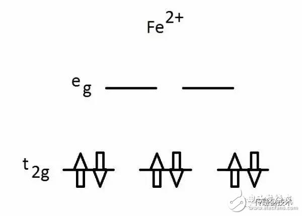
Here is a molecule of iron compound in a 2+ valence environment with a major bond-forming orbital of t2g (low energy) and eg (high energy). According to the incompatibility principle proposed by Pauli, six electron pairs constitute three orbits, and one electron in each electron pair "spins faster" and the other "spins slow down". This is what we call the ground state, also known as the low spin state. Its overall spin value S is equal to 0 because the spin value 1/2 of one electron is offset by the spin value -1/2 of the other electron.
Another mode of this atom is the high-spin state, in which two electrons are transferred to a higher bond orbit, and the overall spin value is S=2:
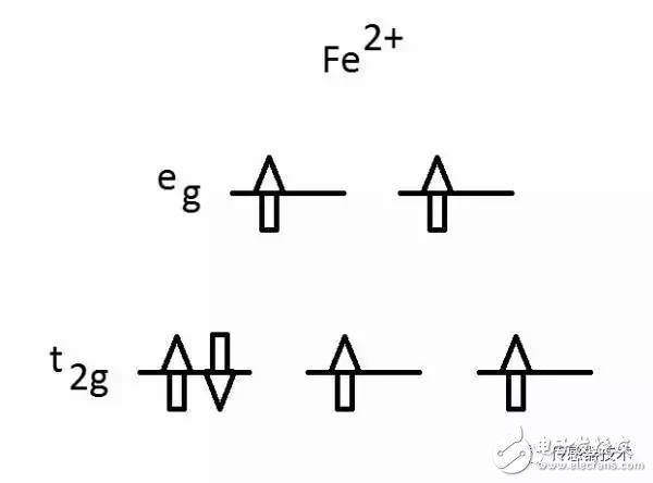
Due to the presence of external stimuli, there will be two electrons flipping the spin and occupying the high energy eg orbit, which is also called the "metastability" state. Depending on the actual arrangement of the surrounding atoms, this state can actually behave very stably, but it is very different in nature from the original ground state.
However, extending this principle to a large amount of material is very difficult in principle. In brief, various research papers indicate that spin-crossing compounds can be directly docked and achieve resistance changes, but most of the papers related to such operations belong to the chemical engineering discipline, and the main researches are carbon nanotubes, graphene layers or organic Objects such as chains.
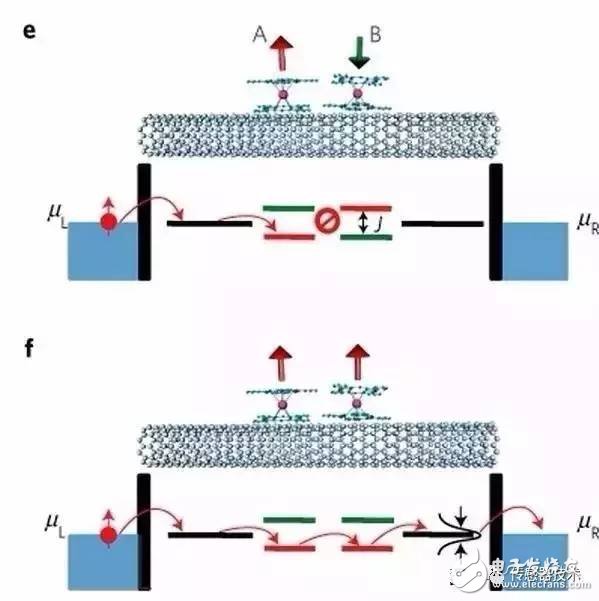
In this paper, the low spin/high spin state will or may not provide conductivity between the two polarities, depending on the actual properties of the metal atoms, electrical resistance, characteristics, and/or platform stability levels. Intel needs to develop a material that can be programmed with voltage changes rather than external stimuli, which obviously takes complexity to new heights.
In general, spin-crossing compounds have a specific temperature window, and their electrons can switch between high and low states at different temperatures, which means that temperature factors have a direct impact on their stability.
From this point of view, the ductility and basic properties of the material become the main obstacle to achieving large-scale spin crossover, especially in the case of simultaneous use of carbon nanotubes. If we want to extend a large amount of metal materials, we need to provide a separate metal environment for batch processing. The line (and gap) will make the original simple track concept more blurred, so we can't incorporate it into it. In the storage unit.
Intel also pointed out that their technology enables each storage unit to carry multiple bits, and the problem of spin-crossing can be solved by using an electronic tunneling mechanism to achieve the goal of building a storage unit.
Spin torque effect (STT for short)
The spin-torque effect of a memory cell depends on the level of resistance between the two states of the cell, plus the ability to control magnetism inside the memory cell. In short, if you adjust the magnetic layout of a material, you can investigate its resistance and use it as a memory.
A more specific explanation is that the long-term existence of the spin torque effect depends on the property called spin-polarized current. From the fundamental point of view, electron spin is divided into two directions, namely spin acceleration and spin deceleration.
The general current is usually uniformly mixed by these two types of directions, so that the whole appears to be in the form of a non-polarized current (ie, there is no overall spin directivity). When a non-polarized current passes through a thick layer of magnetic material, it immediately begins to exhibit polarization characteristics.
If this polarization current then passes through a thin magnetic layer at different electron density states, the polarity of the current will be magnetic, causing more electrons to naturally enter the reverse spin state.
Since the thick magnetic layer has a constant magnetic field directionality, and the thin magnetic layer (or called the free layer) can be flipped (depending on the material itself), the resistance generated by the combination of the two can be used as the memory unit. use.
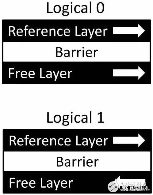
The paper points out that the advantage of the spin torque effect scheme is that its energy consumption level is lower than that of DRAM, but its performance is basically the same as the latter. The obstacles to the implementation of this technology are mainly due to the ability to build permanent magnets with a very small foothold such as nanolithography, plus how to arrange so many tiny magnets in close proximity to each other (similar to the bits in the disk drive). Unit) - This may cause some of them to accidentally flip.
In addition, it is not clear that using this method can provide a capacity of more than a single binary bit per unit. Moreover, existing research indicates that it requires a control transistor to be used simultaneously. Intel has clearly stated that 3D XPoint does not use any control transistors.
The open development history of spin torque effect technology can be traced back to the 1 Mb IC launched by Qualcomm in 2011 and the 64 Mb module from Everspin in 2012, but they have not been put into actual production.
Conductive bridging technology (CB for short)
One of the easiest ways to adjust the path resistance is to physically block the electronic motion path almost completely. Conductive bridging technology (also known as programmable metallization cells) uses a technique similar to electrolysis to create a nanobridge between the electrodes, reducing cell resistance.
Among a conductive bridging unit, a thin electrolyte membrane (which used to exist in a liquid state, but can now also assume a solid state) is between the active and inert electrodes. When the inert electrode is applied with a negative bias, the metal ions in the electrolyte are unwilling to be metal atoms.
When the number of metal atoms precipitated and connected reaches a certain level, it forms a wire between the two electrodes. To cut off this wire, we need to apply a reverse potential difference to reoxidize the atoms in the wire to the electrolyte. The final electrode-electrolyte-electrode combination still has electrical conductivity, but its electrical resistance is higher than in the case of the aforementioned wire.
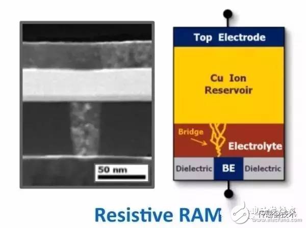
However, for any friend who is familiar with the electrolysis mechanism, the above general description also brings a lot of problems. First of all, perhaps the liquid material is used in the storage unit, but we are more inclined to assume that the mobile ions in the solid material need to be processed, and the active space is between the embedded points (that is, between the lattice/frame). space).
It is worthwhile to carefully scrutinize the word "wire" mentioned in the above expression. In general, atomic precipitation by electrolysis often lacks directivity—we are leading the activity of different crystal faces to initiate precipitation, which leads to ion diffusion in a unidirectional manner, but depending on the actual crystal surface growth, the electrode The pointing will be slightly biased.
In this case, a bifurcation line will appear - similar to the manifestation of lightning. When the different electrodes are connected to each other, or at least within the length of the electron tunnel, the difference in resistance of the wires themselves (from high resistance to low resistance) is also quite large. However, as the wire continues to build, the resistance value will continue to decrease.
With this in mind, the way to create wires does provide multiple bit capacity for each unit, but as I mentioned before, it is quite difficult to implement. Another factor is the process of reversal - usually the same material is used as the ion to provide the active electrode, but this means that the electrode itself is basically also soluble. Through research, we see that this may affect the service life of the product.
In terms of the advantages of the conductive bridging technology, it can theoretically achieve a physical size lower than that of the floating gate unit, and the layout is relatively simple. According to the report, it can be improved by several orders of magnitude in terms of power consumption and performance levels compared to current NAND.
Considering the above problems and advantages, I believe that the conductive bridging technology should be used as the priority object of the 3D XPoint solution. Micron has made relevant hints in the 2002 official license, and the slides presented at the Micron analyst conference in 2014 also mentioned how they overcome some of the issues I mentioned earlier:
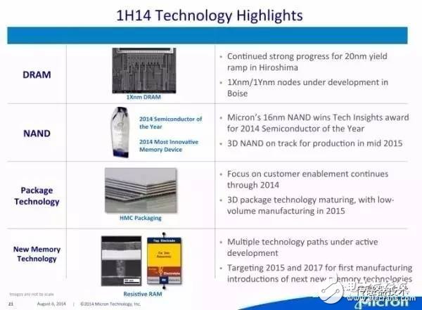
Below the picture is the storage unit that was under development at the time, and the presentation material did mention the existence of bridging technology. To ensure that the active electrode is not "eaten" during reverse programming, the technician sets up a large library of ions for it to call. The other electrode is small in size to allow the wire to be oriented. As long as the entire electrolyte layer is small enough (several monolayers), the read/write operation will be extremely fast and implementation will be very easy.
future development
In summary, if we quickly jump to February 2015, then please pay attention to another demo published by Micron at its analyst meeting:
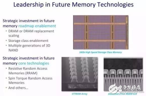
In the lower part of this picture, we can clearly see that Micron is focusing on the memory scheme based on the spin torque effect on the left, and some analysts report that the RRAM cell on the right side of the picture is likely to use Conductive bridging technology. In the 3D XPoint demo released this week, many analysts believe that the most preferred implementation option is likely to use diodes to detect actual resistance characteristics.
Considering that the announcement emphasizes that the ongoing technology research and development is fundamentally different from previous attempts, and the biggest difficulty for 3D XPoint products to enter mass production is manufacturing materials, I can't finally determine which implementation method to use. .
From a probabilistic perspective, Intel and Micron may have used conductive bridging technology to create this product. The most accurate details will be firmly in the hands of Intel and Micron, because after all, the technical progress from concept to product is not easy to advance - considering the aforementioned 2002 release of conductive bridging technology license, the entire study The cycle has continued for a full decade.
According to some pictures given by Intel, the basic unit structure of 3D XPoint is very similar to the current memory chips. They have complete word lines and bit lines, and data is stored between the cross-stacked word lines and bit lines. The specific voltage difference between a word line or a bit line can change the resistance of a particular material. When the data needs to be read, the word line and the bit line can detect the resistance value of a certain storage unit, and feedback the data storage condition according to the resistance value.
3D XPoint FeaturesUnderstanding the basic workings of 3D XPoint seems to be simple. But the actual situation is far more complicated than the one described above. Especially for special voltage differences and specific materials, there is currently no third manufacturer to grasp the principle. Next, let's focus on what changes 3D XPoint can bring to our lives and applications.
Positioning: Not your life and death
According to Intel, 3D XPoint is not a technology for the complete replacement of DRAM and NAND. Its positioning is a new level in computer storage, which can enhance the current storage architecture in different application areas.
From the delay data given by Intel, the read latency of 3D XPoint products is about 10 nanoseconds (the write latency is longer), and there is still a little difference between the minimum DRAM and the nanoseconds of DRAM, but it is far better. At the microsecond level of NAND; in terms of lifetime, the lifetime of 3D XPoint is about one million read and write times, which is several orders of magnitude higher than the thousands of reads and writes of MLC in NAND. Of course, it is still incomparable with DRAM; bandwidth On the other hand, the application of multi-channel technology makes 3D XPoint not have any disadvantages in terms of bandwidth.
In Intel's official publicity, 3D XPoint has similar NAND-like capacity and DRAM-like performance. Including faster than NAND (should mean low latency) more than 1000 times, life expectancy is more than 1000 times NAND, data density is more than ten times that of DRAM.
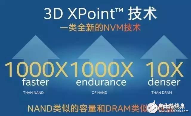
â–² 3D XPoint performance is very good.
Intel believes that such performance allows users to choose a new combination of storage systems based on different needs, such as DRAM+3DXPoint+NAND three-level storage system, or 3D XPoint to take over DRAM+NAND, or DRAM+3D XPoint's solution can even be a 3D XPoint+NAND system. The cost, focus and performance of different solutions are different. The ending is open, and there is no impetus to replace who, but according to the market choice to match Program.
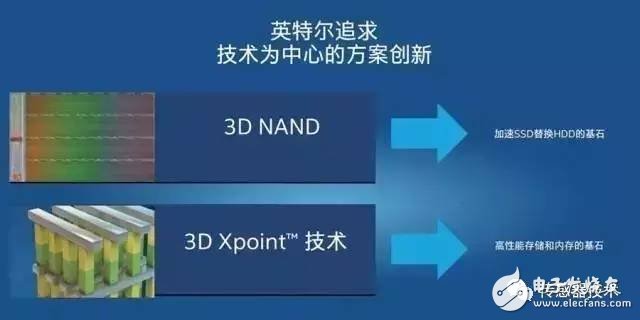
â–² NAND and 3D XPoint is not a competitive relationship between you and me.
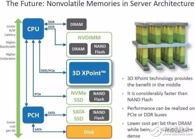
â–² 3D XPoint's position in the system.
Lifetime: competent for all hot temperature storage scenarios
The life-related problem is actually the most discussed in NAND applications, because TLC's NAND chip can exhaust all the life of a unit in a thousand-level full read and write. Thousands of times sounds very short, but a large number of data centers and enterprise users have deployed NAND storage devices. This proves that the life of NAND is better solved with the help of various average friction and data buffer algorithms. In our previous tests, the SSD of the TLC chip was also not a problem under stress testing.
Compared to NAND, the life of 3D XPoint is actually not a problem. According to Intel data, if 3D XPoint has 2 million read and write life, under the balancing algorithm, a 512GB 3D XPoint device theoretically needs to completely read and write 1024PB to die, which is equivalent to writing 574TB data every day for five years. In addition to special occasions where DRAM must be used to maintain ultra-high loads, 3D XPoint is fully qualified for almost all current hot/temperature storage center applications. As for cold storage, it has not been suitable for the latest high-speed storage devices from a cost perspective.
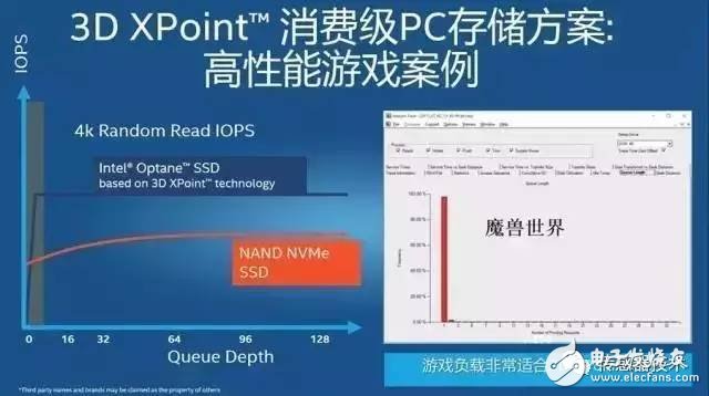
â–² 3D Xpoint is also useful on high-performance consumer PCs, and the IOPS throughput speed is extremely fast at all queue depths.
Price: not too cheap
Speaking of the price of 3D XPoint, we need to consider two aspects: one is cost, and the other is market positioning.
Look at the cost first. According to data presented by Intel and Micron, 3D XPoint's single die can cut 396 3D XPoint die, each with a die area of ​​approximately 210 square millimeters (128Gb per die). In contrast, a 20 nm 128 Gb MLC NAND die has an area of ​​approximately 202 square millimeters.
In general, apart from other costs in R&D and production, from the perspective of the wafer, the cost of 3DXPoint should be similar to that of NAND. Of course, the yield is another.
Next look at the market positioning. In general, the market position of a product is determined by its performance location in the market. At present, the performance of 3D XPoint is positioned under DRAM and above NAND, but it is more DRAM-oriented, so it should have similar market positioning. Considering the current price of DRAM, it can be said that the price of 3D XPoint should not be too cheap.
On the other hand, Intel itself has a huge NAND factory and a small market share. 3DXPoint will not grab the NAND rice bowl at this time in terms of technical and commercial interests. And if it is divided from the enterprise level and the consumer level, by convention, after the product matures, Intel will obviously be more inclined to apply this new technology to the enterprise products with higher profits.
The utility model discloses an Electronic Cigarette with atomizer oil core separation structure, which comprises a atomizer assembly and a battery assembly; The utility model has the advantages of reasonable structure design and high practicability. During operation, because the oil storage tank of the atomizer is completely sealed and the oil guide material is completely isolated from the oil guide material, the oil guide material will never contact with the oil guide material in the storage process
Advantages:
Oil core separation, Mesh removable heating core, Ultra quiet design,100% oil leakage free, Excellent taste, Cost far less than the industry price.
A variety of colors and finishing are available, can be adjusted according to your market needs.
Oil Coil Separation Pod Patent,Oil Coil Separetion Vape Pod Oem,Innovated Vape Products Oem,Oil Coil Separation Vape Products Oem
Shenzhen MASON VAP Technology Co., Ltd. , https://www.e-cigarettefactory.com