Lattice Semiconductor White Paper
introduction
With the rapid growth in the use of sensors, low-cost cameras and displays in today's embedded designs, there are many exciting new smart and visual applications on the market. At the same time, the explosive development of embedded vision applications has given design engineers a new understanding of the need to handle resources. New video applications with rich data are driving design engineers to rethink which device is being used, is it a dedicated application processor (AP), ASIC, or ASSP? However, in some cases, the large amount of software investment in existing application processors, ASICs, or ASSPs and the high startup cost of new devices have become a hindrance to the above-mentioned application update iterations. This time, the issues at hand are driving design engineers to look for a co-processing solution that not only provides the extra functionality needed for new applications with rich data, but also meets the stringent requirements of system cost and power consumption.
In addition, the widespread adoption of low-cost MIPI peripherals for mobile applications on the market has created an interconnection challenge that has never been seen before. Design engineers want to take advantage of the mass production cost of the latest generation of MIPI cameras and displays, while hoping to retain investment in traditional equipment. So in this fast-moving environment, how do design engineers address the emerging interface mismatch between sensors, embedded displays, and application processors?
Design engineers need a highly flexible solution that delivers a high-performance, "best-in-class" coprocessor that meets the needs of both visual and intelligent applications for logic resources and highly parallel computing power, while adding to the variety of I/O Interconnection support for standards and protocols. In addition, such a solution should have a highly scalable architecture and support low-cost external DDR DRAM using mainstream high data rates. Finally, the solution needs to be optimized for low-power and low-cost computing, and provides design engineers with an industry-leading ultra-small package.
In this article, we'll show you how ECP5TM and LatticeECP3TM FPGAs enable co-processing and interconnect solutions for embedded designs, with a focus on application examples for these solutions in industrial, consumer, automotive and machine learning.
Efficient co-processing solutions for vision and smart applications
Lattice Semiconductor®'s ECP5 and LatticeECP3 FPGA families enable the "best in class" coprocessor and are optimized for interconnect functionality as well as high performance and low power. The ECP5 FPGA family offers the industry's smallest package (10x10 mm) and up to 85K look-up tables (LUTs), which are nearly twice as powerful as competing products, while reducing cost and power consumption. ECP5 FPGAs support interoperability with ASICs, ASSPs, and application processors with optimized I/O and architecture. Enhanced embedded DSP blocks and highly parallel FPGA logic architectures provide the high performance support required for compute-intensive co-processing functions. The ECP5 FPGA family offers up to four SERDES interconnect channels supporting PCI Express (Gen1, Gen2), Ethernet (1GbE, SGMII, XAUI), CPRI, embedded display port (EDP) and JESD204B at 250 channels per channel Mbps to 5 Gbps. At the same time, the programmable I/O on the device supports various interfaces including DDR3, LPDDR3, LVCMOS, RGMII, XGMII, LVTTL, LVDS, Bus-LVDS, 7:1 LVDS, LVPECL and MIPI D-PHY.
Design engineers can choose a LatticeECP3 FPGA when a co-processing or interconnect application requires more than 85K LUTs or more than four SERDES channels. The LatticeECP3 FPGA family offers up to 150K LUTs and 6.8 Mbit SRAM in packages down to 10x10 mm. This family supports up to 16 3.125 Gbps SERDES channels compared to the ECP5 FPGA family. In addition, the devices in the family support 800 Mbps DDR3 and LVDS, and can provide more than 500 programmable system I/O buffers, support Ethernet (via RGMII and XGMII), and a large number of additional I/O interfaces. Embedded SERDES supports PCIe, Ethernet (via SGMII and XAUI), HDMI, High Speed ​​Serial I/O (Serial Rapid I/O), CPRI, JESD204A/B and more. The LatticeECP3 FPGA family consumes as little as 0.5 W. Like the ECP5 FPGA family, design engineers using LatticeECP3 FPGAs can efficiently perform computationally intensive functions using highly parallel FPGA logic architectures and share vision and intelligence functions such as image processing and analysis tasks to reduce processor workload through FPGAs. This results in lower power consumption and higher performance.
Implement vision processing solutions for industrial applications
In the industrial world, ECP5-based FPGA co-processing can play an important role in reducing the computational load of application processors, ASICs, or ASSPs in video camera, surveillance, and machine vision applications. Figure 1 shows a typical industrial camera application. In the illustration below, the FPGA is located between the image sensor and the Ethernet PHY. The image sensor streams the image data to the FPGA, which then performs image processing or image compression based on H.264 encoding. The FPGA's on-chip Embedded Block RAM (EBR) and DSP blocks enable high performance wide dynamic range (WDR) and image signal processing (ISP) functions. Finally, the FPGA transmits the image data over Ethernet.
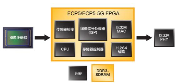
Figure 1: ECP5 FPGA reduces the computational load of the application processor in industrial camera applications by implementing image processing or compression
In addition to image processing and compression, if the type or number of application processor interfaces does not match the camera or sensor, the FPGA can also be used to implement video bridging between them. To meet the demand for flexible interconnects in industrial applications, Lattice has introduced programmable ECP5 12K devices that can be connected to common interfaces including LVDS, MIPI and LPDDR3. The device provides the logic, memory and DSP resources required for pre- and post-processing functions in applications such as LED controllers, machine vision systems and industrial motor control at low cost.
In addition to common industrial camera applications, machine vision (a more specialized camera application in the industry) can also benefit from the interconnect and co-processing capabilities offered by ECP5 FPGAs. The block diagram in Figure 2 shows the many roles FPGAs can play in common industrial machine vision systems. In camera applications, FPGAs can be used to implement sensor bridging, complete camera ISP or custom functions to help system designers achieve differentiated end products. For image acquisition cards, FPGAs like ECP5 can solve video interface problems and implement image processing functions.
Machine vision system block diagram
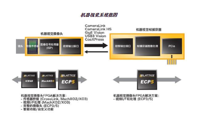
Figure 2: FPGAs can be used to implement various interface bridging and processing functions in common industrial machine vision solutions
Intelligent traffic and surveillance camera applications for smart cities
Intelligent Transportation Systems (ITS), including traffic flow monitoring, traffic violation identification, smart parking and toll collection, are important components of smart cities. The above systems usually require an intelligent traffic camera for accurately detecting information on various aspects of the vehicle, such as license plates, and performing video analysis at the edge of the network even in a hostile environment without sending the original video stream back to the cloud for processing. A single application processor typically cannot meet both system power consumption and real-time processing requirements. The low-power, small-footprint ECP5 FPGA family can be used as a coprocessor for application processors to achieve the efficient real-time processing required by the system at the edge of the network.
In addition to the ISPs mentioned above, ECP5 FPGAs can also implement video analytics to further reduce the computationally intensive tasks of the application processor, thereby reducing system power consumption and achieving higher real-time performance. FPGAs enable solutions for target detection, image processing and image enhancement for smart camera applications. For example, the detection target may be a face image in a surveillance camera instance or a license plate in a traffic camera instance.

Figure 3: ECP5 FPGA implements image processing and video analysis functional block diagrams for smart camera applications, sharing the computationally intensive tasks of the application processor
In the example of the intelligent traffic camera shown in Figure 3, the FPGA detects the vehicle license plate based on the image data captured by the sensor, and can perform image enhancement to generate a clear image even under low light or strong backlight conditions - for the target (license plate) and background (The rest of the image) uses different exposure settings and then blends the target and background images to produce a sharper image. Then, the target detection result generated by the FPGA is input to an analysis algorithm run by the application processor. Using the parallel processor architecture of the ECP5 FPGA to share the most computationally intensive steps in the analysis algorithm, the smart camera can improve performance while maintaining low power consumption.
Implement immersive augmented reality (AR) and virtual reality (VR) applications for mobile systems
As AR/VR market demand continues to grow, current head-mounted display (HMD)-based systems face the problem of insufficient performance when mobile application processors run content. Therefore, the vision-based location tracking required to achieve an immersive AR/VR experience is challenging for the processor. In this case, the EPC5 FPGA's efficient parallel processing architecture is ideal for implementing position tracking solutions based on stereo cameras and LED markers. FPGAs offer low-latency, low-power image processing support compared to application processors. The programmable architecture and I/O of the FPGA also allows system designers to easily select image sensors from different vendors based on product requirements.
In the "outside-in" location tracking solution, the stereo camera is placed in the room (seeing the user in the indoor camera), tracking the user's movements (such as the body by capturing the LED markers mounted on the user's helmet and handle controller) Exercise and hand movement), as shown in Figure 4 below. The FPGA installed inside the camera unit on the tripod calculates the user's position, body and hand movements based on the data captured by the stereo camera, and then wirelessly transmits the data to the mobile application processor in the user's helmet, finally through the AR/VR application. Presenting the interaction between the real world and the virtual world. The stereo camera provides depth-aware support for algorithms running on the FPGA to achieve three-coordinate positioning.

Figure 4: The “outside-in†position tracking solution using a stereo camera (placed in the room) to track the user's body and hand movements by capturing LED markers mounted on the user's helmet and handle controller
In the "inside-out" location tracking solution, a stereo camera mounted on the user's helmet (from the user's location "inside-out" toward the indoor environment) captures the LED markers mounted on the handle controller to track The user's hand movements are shown in Figure 5. The FPGA installed in the user's helmet camera unit calculates the user's hand motion based on the stereo camera data, and then sends the data to the mobile application processor in the helmet, which is finally presented by the AR/VR application.

Figure 5: "inside-out" position tracking using a stereo camera (mounted on the user's helmet) to track user hand movements by capturing LED markers mounted on the handle controller
While both "outside-in" and "inside-out" tracking solutions provide an immersive experience, the "outside-in" system provides greater immersion because it can also be tagged with LEDs on the helmet Track body movements (such as walking, running, squatting, jumping, etc.) and map physical movements in the real world to the virtual world.
In both systems, the user's motion information needs to be presented in the virtual world immediately with very low latency for the most realistic user experience. The parallel processing power of the ECP5 FPGA is the key to achieving low latency transmission. In addition, its low power and small package features are key to achieving an unobstructed mobile experience.
Co-processing and bridging solutions for automotive ADAS systems
The automotive market for visual processing and interconnection solutions? The demand for the 6?7?6?7 case is growing substantially. Analysts at IC Insights, a market research firm, expect to implement the new regulations for rear-facing cameras in a new generation of automotive designs and the introduction of cameras in automotive designs to replace the two-sided rearview mirrors for blind spot detection and lane tracking. With the development trend, CMOS image sensors will grow at a compound annual growth rate of 55% from 2015 to 2020 with the rise of new applications in the automotive field.
In this fast-growing market, automotive design engineers need solutions that not only enable pre- and post-processing capabilities, but also build optimized interconnect solutions for advanced driver assistance systems (ADAS) and infotainment applications. 6?7?6?7 case. As ADAS systems developed by automakers become more complex, design engineers face two major challenges. The first challenge is how to solve the interface problem caused by the growing number of cameras? Most modern processors have only two camera interfaces, and many ADAS systems require up to eight cameras to meet evolving autopilot requirements. The second challenge is how do design engineers perform image processing based on large amounts of data from the above cameras?
To meet these challenges, design engineers need a solution that provides co-processing resources that stitch together multiple streams of video from multiple cameras or image processing inputs from multiple cameras (such as white balance, Fisheye correction, defogging), and then transfer this data to the application processor through a single data stream. Automotive design engineers also need the flexibility to operate multiple displays on dashboards, dashboards, and rear seat infotainment systems, as well as bridge between traditional interfaces and new MIPI interfaces.
The Lattice Automotive Grade ECP5 FPGA (AEC-Q100) provides the parallel processing power required to accelerate the image processing pipeline for these applications, while the large number of I/Os can be used to connect to larger camera arrays. An example of this trend is that more and more cars now have bird's eye view capabilities. In general, the bird's eye view function refers to a live video image looking down from 20 feet above the car. The ADAS system does this by stitching together data from four or more cameras to achieve wide field of view (FoV).
Design engineers have traditionally used a single processor to process image data from a single camera. Design engineers can now replace multiple processors with a single ECP5 FPGA, aggregate data from multiple cameras, and perform image stitching, fisheye removal, white balance, HDR adjustments, etc. to maximize image quality and then high quality The image is sent to the processor for the next step. Designers using this approach can achieve higher performance while reducing cost and power consumption.
Figure 6 shows how Lattice customers can build the solution mentioned above. The bird's eye view system captures video images from cameras (front, rear, and sides) mounted around the car. The ECP5 FPGA is used to continue processing and stitching the video data to provide a 360 degree view. In this case, a single FPGA can replace multiple ARM processors. The system finally presents a clear 1080p 60 fps video. In addition to the ECP5 FPGA, this solution uses only a low-end ARM processor for initial calibration and video encoding/recording.
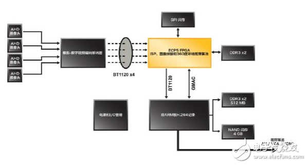
Figure 6: Shows how a development engineer can use a single ECP5 FPGA to implement a bird's eye view system that previously required multiple ARM processors.
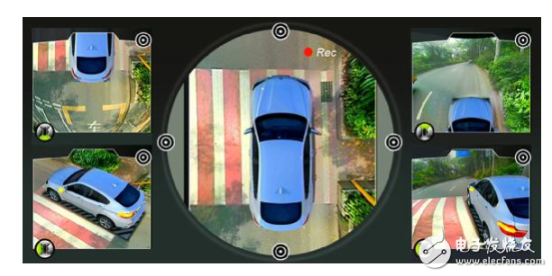
Figure 7: Shows a 360-degree panoramic view of the ECP5 FPGA using image input from 4 cameras
Another important role that FPGAs can play in automotive design is to build a low-cost bridging solution between traditional interfaces and the increasingly popular MIPI camera and display.

Figure 8: In an in-vehicle infotainment system, ECP5 FPGAs can be used for pre- and post-processing functions and enable video bridging between the application processor and the display
For example, in the block diagram of Figure 8, the ECP5 FPGA is located between the application processor or SoC and one or more automotive displays for pre- and post-processing functions and implements DSI or FPD-Link interface application processors and Open Bridging between LDI, LVDS, FPD-Link, or eDP interface displays. FPGAs can also be used in a variety of other infotainment applications, including separately outputting a single video to a dual rear-seat display, cropping and formatting the image to achieve a specific video resolution.
ECP5's rich processing resources also lay the foundation for a variety of sensor bridging, aggregation and co-processing solutions. As shown in Figure 9, the ECP5 FPGA is used to control and aggregate intelligent centers from multiple sensor data. By pre-processing and post-processing sensor data and implementing I2C management functions and SPI interfaces, FPGAs can significantly reduce the computational load on the application processor.
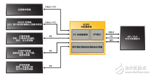
Figure 9: ECP5 FPGA implements data bridging and smart center for controlling and aggregating multiple types of sensors
Another example of bridging, aggregation, and co-processing solutions uses Lattice's 3.2 Gbps SERDES capabilities for automotive-grade FPGAs to aggregate data from multiple radars or cameras and pass through an automotive internal network such as BroadR-Reach or Ethernet? 6?7?6?7 transmission. In Figure 10, data from multiple sensors is transmitted to the ECP5 FPGA via the LVDS interface, which then aggregates and packs the data and transmits it to the vehicle's internal network via the SERDES-based SGMII interface.

Figure 10: LVDS and 3.2 Gbps SERDES for automotive-grade ECP5 FPGAs for bridging and aggregation of multiple radars or cameras and transmission to the in-vehicle network via SGMII
Implement network edge machine learning applications
Looking ahead, the impact of mobile-related solutions will continue to grow, and they will continue to leverage the application support and scale manufacturing advantages of mobile processors and MIPI sensors and displays to enable intelligent functions at the edge of the network. There is a growing demand in the market for deploying artificial intelligence (AI), neural networks, and machine learning to achieve these goals.
In machine learning applications, neural networks for image recognition can be trained to recognize cat images, for example by feeding thousands of images to the neural network and assigning input image weights until the neural network is correct. Identify the image of the cat. Developing data architectures and assigning weights can require terabytes of data and a large amount of computing resources. Therefore, the training steps of machine learning applications based on deep learning technology are placed in data centers using high-end GPUs and FPGAs, and only a large amount of computing needs in the data center can be met.
Once the model is trained, it will be ported to an embedded system in a network edge application and then implemented for reasoning functions for applications such as image recognition or speech recognition. In the field of network edge applications, devices must make decisions faster and more efficiently through calculations. Therefore, the design engineer needs to apply the lessons learned in the “training†phase of the neural network to the new data and “infer†to the results. In order to implement inference functions in the field of network edge applications, the ideal solution is to provide a highly computationally efficient platform that meets the stringent requirements of power consumption, size and cost.
Today's industry and academia believe that machine learning requires a highly specialized hardware acceleration solution. However, the requirements will vary depending on the task. For example, training and reasoning may require different hardware. Hardware design engineers working on training applications typically use 32-bit floating-point operations for very high-precision calculations. On the other hand, hardware design engineers working on inference functions in the field of network edge applications need more flexibility than precision in order to achieve higher processing speed or lower power consumption. In fact, recent research has shown that for many applications, fixed-point and floating-point solutions are almost identical in terms of inferential accuracy, and the former consumes less power.
With a rich set of embedded DSP resources, FPGAs and an inherent parallel processing architecture, as well as significant leadership in power, size and cost, ECP5 FPGAs are ideal for meeting the diverse needs of the emerging AI market. For example, a DSP in an ECP5 FPGA can perform fixed-point operations at a lower power/MHz than GPU floating-point operations. These features provide an attractive advantage for power-demanding network edge intelligence solution developers. Figure 11 shows an example in which the ECP5 FPGA is used to implement an inference accelerator that processes pre-trained convolutional neural networks (CNNs) from data from the camera. The CNN engine running on the FPGA recognizes objects or faces and sends the results to the system CPU for fast, low-power object/face recognition.

Figure 11: ECP5 FPGA implements Convolutional Neural Network (CNN) Accelerator for Network Edge Intelligence Applications for Object/Face Recognition
The block diagram in Figure 12 shows a real-time face tracking neural network acceleration demonstration that consumes only 0.85 W when running on an ECP5-85 FPGA with an 85K LUT.
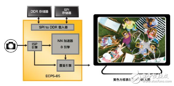
Figure 12: Real-time image data captured by the camera is input to the FPGA, the FPGA determines the face image and outputs the result, and finally the face image is highlighted on the display.
FPGA-based design allows designers to flexibly scale up or down to meet the power and performance balance of end systems. In the above example, the design based on the smaller size of the 85K LUT FPGA can be achieved by balancing performance and other parameters such as reducing the frame rate, reducing the frame size of the input image, or reducing the weight and activation values ​​for the neural network. To further reduce power consumption.
In addition, the reprogrammable nature of FPGAs enables design engineers to meet rapidly changing market demands. As the algorithm evolves, users can easily and quickly update hardware through software. This is a feature that GPUs or ASICs can't match.
The above demonstration is based on the Embedded Vision Development Kit (Figure 13), part of the Lattice Embedded Vision Solutions portfolio, which provides a modular platform for developing network edge embedded vision solutions.
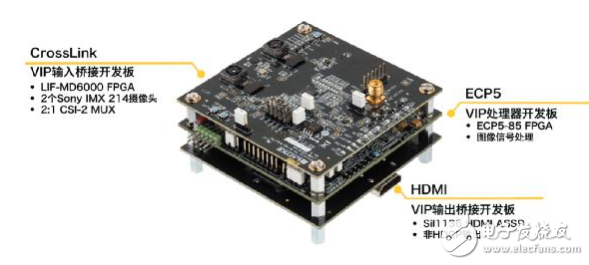
Figure 13: Lattice Embedded Vision Development Kit with ECP5 FPGA, CrossLink FPGA and HDMI ASSP
to sum up
Today's design engineers need to constantly find new ways to reduce the cost, power, and size of their designs while enabling more intelligence for network edge applications. At the same time, they have to keep up with the performance and interface requirements of the rapid development of next-generation sensors and displays in network edge applications. The Lattice ECP5 FPGA family offers design engineers the best of both worlds. ECP5 FPGAs offer superior processing power (up to 85K LUTs) and the industry's smallest package (10x10 mm) with SERDES to provide design engineers with the co-processing and interconnect resources they need. At the same time, the product line has lower cost and power consumption than competing products, which can give development engineers a leading edge.
Gold Room Switch And Socket,Gold Double Light Switch,Gold Homekit Light Switch,Dimmer Switch
ZHEJIANG HUAYAN ELECTRIC CO.,LTD , https://www.huayanelectric.com