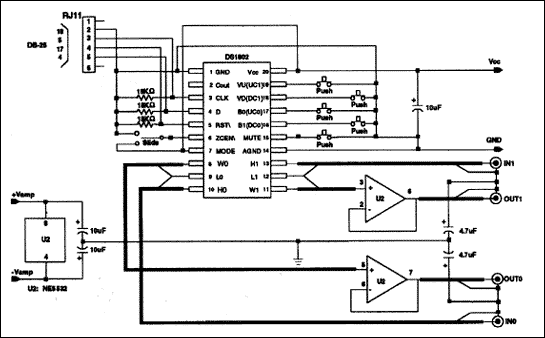
Figure 1. Test configuration circuite.
Several steps were taken to minimize the effects of extraneous noise on measurement data. Shielded cabling was used on all inputs and outputs from (or to) the DS1802 and NE5532 Op Amps. All ground signals were tied to a common point and power supplies were capacitively coupled to ground using 10 µF capacitors. Additionally, both the DS1802 and NE5532 Op Amps used separate power supplies.
Once assembled, this circuit was mounted inside a metal testbox to provide additional protection against coupling of random noise from external sources such as computer monitors, lights, etc. BNC connectors were used for inputs and outputs to test equipment.
Test Measurement EquipmentAudio measurements were performed using the Audio Precision-System One A version audio analyzer under PC-control. This test equipment provided the means of measuring THD + N, IMD, cross-talk, absolute error, and inter-channel matching. Test Measurements PerformedAs stated in the scope of this document, device tests were completed on absolute error between tap points, inter-channel matching, THD + N, IMD, cross-talk, mute-levels, and device current characteristics as a function of temperature . These tests and data are presented in the following pages of this section of the report. Absolute Error and SummaryAbsolute error is defined as the difference between the expected voltage output and the measured voltage output at a given wiper position. The DS1802 is specified to provide an absolute tolerance of ± 0.5 dB for any given wiper position. For example, wiper position 48 would be expected to provide -48 dB ± 0.5 dB of signal attenuation difference relative to wiper position 0 (or the input signal if connected to the high-end terminal of the potentiometer).Graphical data is presented in Figures 2 and 3 for a sample set consisting of five units of the DS1802. Figure 2 presents actual data for the five devices tested. Figure 3 further summarizes this data by presentation of the calculated average. The absolute error data taken in these tests indicate the DS1802 performs well within specified data sheet limits of ± 0.5 dB.
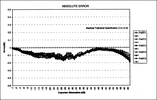
Figure 2. DS1802 Absolute error.
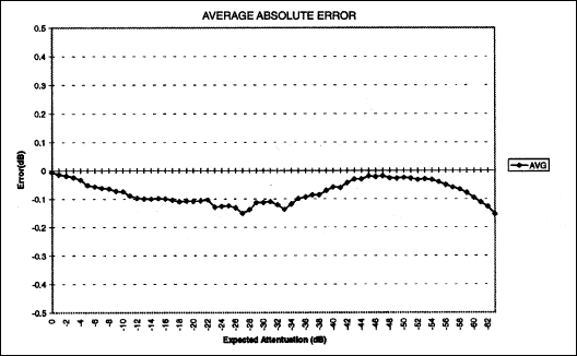
Figure 3. DS1802 Average absolute error.
Figure 4 provides actual data taken on the units, while Figure 5 shows a summary of the average data. Average data for inter-channel matching indicates that this device characteristic falls within a ± 0.05 dB window; which is well within the data sheet specification of ± 0.25 dB.
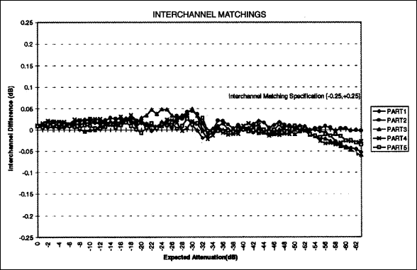
Figure 4. Inter-channel matching.
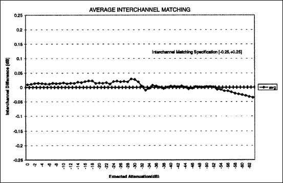
Figure 5. Inter-channel matching summary.
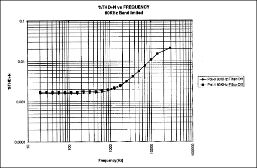
Figure 6.% THD + N vs. Frequency 80kHz bandlimited.
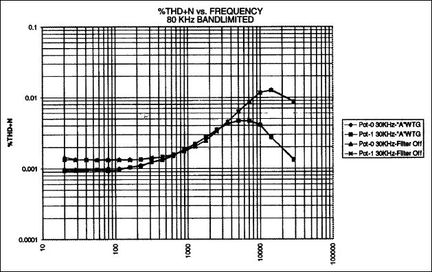
Figure 7.% THD + N vs. Frequency 30kHz bandlimited.
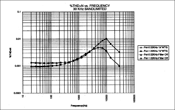
Figure 8.% THD + N vs. Frequency 22kHz bandlimited.
By setting the wiper position of the potentiometer at some level other than position-0 allows the potential user of the DS1802 to view distortion of the part as the input signal covers some portion of the resistor array. A position setting of 0 primarily allows the examination of the input signal source. The position-6 setting used in these tests provides a worst case selection for monitoring% THD + N.
The DS1802 is specified for a% THD + N of 0.002% at 1kHz. This specification is derived using the 80kHz bandlimited input signal at 1Vrms, and a position-6 potentiometer setting. Across the 20Hz to 20kHz frequency range% THD + N is less than 0.02% maximum with the 80kHz bandlimited signal. Additionally,% THD + N across the 20Hz to 20kHz frequency range is significantly improved using bandlimited signals in conjunction with the A-weighting filter.
The A-weighting filter is a specific noise weighting filter (ANSI S1.4, IEC Recommendation 179) used to produce noise measurements which correspond well with human observations over the audio frequency range. 1 More detailed information concerning this filter can be found in the ANSI specification stated above or in the Audio Measurement Handbook published by Audio Precision, Incorporated.
Intermodulation Distortion (IMD) Intermodulation distortion data is provided for the SMPTE and the CCIF intermodulation measurement standards. Data is presented as a function of amplitude for each measurement technique and is shown in Figures 9 (for SMPTE) and 10 (for CCIF).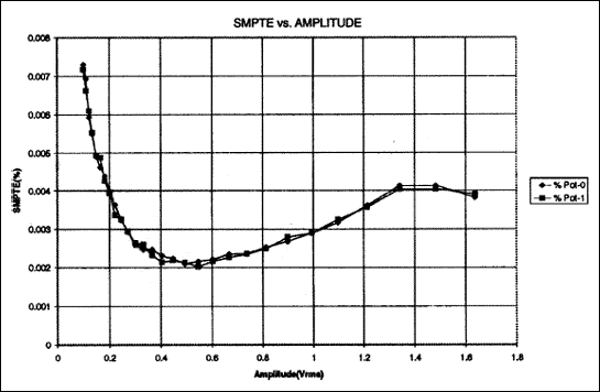
Figure 9. SMPTE Intermodulation distortion vs. amplitude.
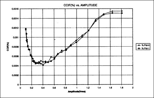
Figure 10. CCIF Intermodulation distortion vs. amplitude.
The SMPTE (Society of Motion Picture and Television Engineers) standard specifies a two-sinewave test signal consisting of a low-frequency, high-amplitude tone linearly combined with a high-frequency sinewave at 1/4 the amplitude of the low-frequency tone . The SMPTE specification calls for 60Hz and 7kHz as the two sinewaves. When a non-linear device is subjected to a two-tone test signal, intermodulation products appear as sidebands around the high-frequency tone. The percentage intermodulation distortion is defined as the percentage of amplitude modulation, represented by the second and third order pair of sidebands, of the high-frequency signal. Second order sidebands around the high frequency tone are spaced at a frequency equal to the low-frequency tone (FH ± FL). Third order sidebands are spaced at twice the low-frequency tone or FH ± 2FL. (FH and FL correspond to the highfrequency and low-frequency tones, respectively. 2)
CCIF intermodulation distortion testing consists of using two equal-amplitude, high-frequency signals spaced closely in frequency. Signals used for test data presented include 13kHz and 14kHz. The audio analyzer measures only the amplitude of the difference tone or low-frequency product resulting from the two high-frequency test signals. Here, the percentage intermodulation distortion is defined as the percentage of amplitude modulation which the low order or difference signal (FH-FL) represents on the high-frequency signals. Additional information on SMPTE and CCIF can be found in the Audio Measurement Handbook and System One Audio Analyzer User's Manual published by Audio Precision, Incorporated.3
Cross-TalkCross-talk measurements were performed using the test configuration diagrams of Figures 11 and 12. The cross-talk analysis is performed by evaluating signals taken from both wipers of the DS1802. In this test, potentiometer 0 is supplied a signal from the Audio Precision analyzer. This signal is returned to the analyzer via the wiper of potentiometer 0 (view either Figure 11 or 12). This signal return is connected to the audio analyzer's channel-A input.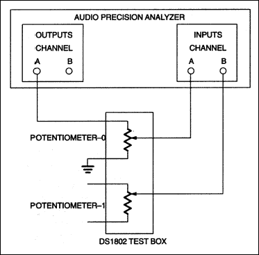
Figure 11. Cross-talk configuration potentiometer 1 open.
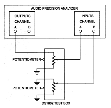
Figure 12. Cross-talk configuration potentiometer 1 grounded.
Potentiometer 1 and its wiper (primarily the wiper) are used as the comparison point for signal feedthrough. The high and low terminals, H1 and L1, are either left open circuited, as shown in Figure 11 or grounded as shown in Figure 12. The wiper of potentiometer 1 is connected to the audio analyzer's input via channel-B.
A comparison between the channel-A input and channel-B input of the audio analyzer is then made to determine the level of cross-talk. Graphical data of both the configurations of Figures 11 and 12 are presented in Figure 13.
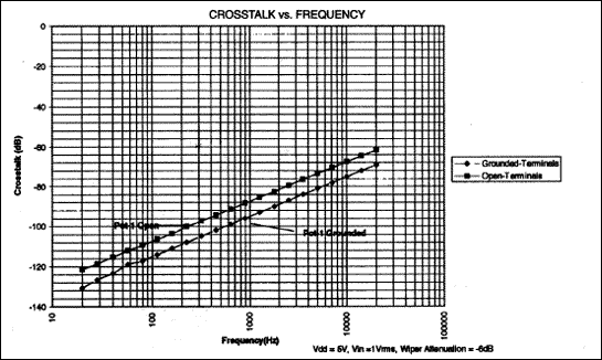
Figure 13. Cross-talk data.
As can be seen from graphical data, temperature has little or no effect on absolute tolerance.
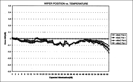
Figure 14. Wiper position vs. temperature potentiometer 0.
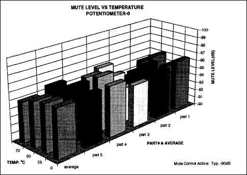
Figure 15. Device muting level—potentiometer 0.
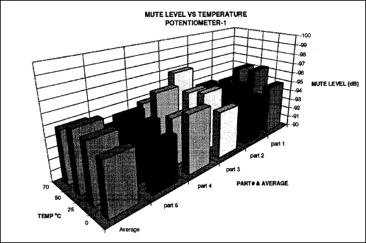
Figure 16. Device muting level—potentiometer 1.
For information concerning pushbutton inputs or zero-crossing detection mode, refer to the data sheet of the DS1802.
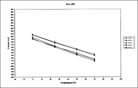
Figure 17. Active current vs.temperature.
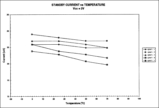
Figure 18. Standby current @ VCC = 3 volts.
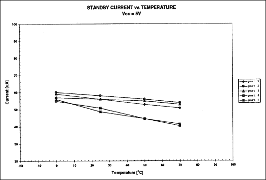
Figure 19. Standby current @ VCC = 5 volts.
Questions concerning this report or data provided in this report can be directed to 214-450-8167
Bibliography Bob Metzler, Audio Measurement Handbook, 1st edition, (Beaverton, Oregon: Audio Precision, 1993), p. 147. Bob Metzler, Audio Measurement Handbook, 1st edition, (Beaverton, Oregon: Audio Precision, 1993), p. 37 -39. Audio Precision, User's Manual Audio Precision System One, 15th Revision, (Beaverton, Oregon: Audio Precision, November 1992), Chapter 16.Via In Pad PCB
What is Via In Pad? In shortly,via in pad is the via holes are at the SMD pad.The vias are very small,usually under 0.3mm.Why and how? First is there is no enough space to layout,you have to put the vias and holes closer even together.Second it helps thermal management and for high frequency boards,it may help improve signals.
Because the SMD pads are for SMD components loading,so the solder can not flow to inner layer or the other side when assemble.That is the most important for via in pad board.
How PCB manufacturers like us to do via in pad board? We will fill all vias with non-conductive epoxy and plate copper over it ,so the vias are flat same as others. Many PCB factories are unable to do such capability.
The key technology is how we fill vias and guarantee there is no any solder (surface finishing) in the holes.
Filled via in pad is a way to achieve intermediate density with an intermediate cost compared to using blind/buried vias. Some of the key advantages associated with using the via in pad technology are:
.Fan out fine pitch (less than .75mm) BGAs
.Meets closely packed placement requirements
.Better thermal management
.Overcomes high speed design issues and constraints i.e. low inductance
.No via plugging is required at component locations
.Provides a flat, coplanar surface for component attachment
Via in big pads are not a big problem.but for BGA,that is technology.As BGA pads are very small,10mil or 12mil,and there is no enough space.Manufacturing is not easy as other boards.
Via In Pad PCB
Via In Pad PCB,6Layer Via In Pad PCB,Touch Pad PCB,Via In Pad
Storm Circuit Technology Ltd , https://www.stormpcb.com