introduction
Digital filters play an important role in applications such as speech and image processing, pattern recognition, radar signal processing, and spectrum analysis. It can avoid the problems of temperature drift and noise that cannot be overcome by the analog filter. At the same time, it has higher accuracy, better stability, smaller size, and more flexibility than the analog filter, so it is widely used. In sonic logging, it is usually necessary to accurately filter the signal, and the filter has strict real-time requirements. This paper uses the auxiliary Matlab design tool to design a high-order fast digital filter based on FPGA that can meet logging requirements.
1 Linear phase FIR filter structureThere are many types of digital filters, and the classification methods are also different. From the point of view of the unit impulse response of digital filters, digital filters are divided into finite impulse response digital filters (FIR) and infinite impulse response digital filters (IIR). Compared with the IIR filter, the FIR filter can carry out accurate linear phase design, and its structure has stable quantization filter coefficients. For acoustic logging processing of acoustic signals with linear phase requirements, FIR filters are the first choice.
In the time domain, the input and output process of the FIR filter is a process of linear convolution between the input signal and the unit impulse response. The expression of the difference equation is:

Among them, y (n) is the filtered output, x (n) is the sampled data, and h (n) is the filter tap coefficient. Its structure is shown in Figure 1(a). In the figure, the N-1 order FIR filter needs to be described by N coefficients. Generally, N multipliers and N-1 two-input adders are needed to realize it. It is not difficult to find that the coefficient of the multiplier is exactly the coefficient of the transfer function, so this structure is also called a direct structure.
For FIR linear phase filters with symmetric coefficients, equation (1) can be written as follows:

The structure of the improved FIR filter with symmetrical coefficients is shown in Figure 1(b). This structure combines the taps with symmetrical coefficients (same or opposite) and then performs multiplication. This reduces the number of multipliers to half of the original number, but also adds additional adders.
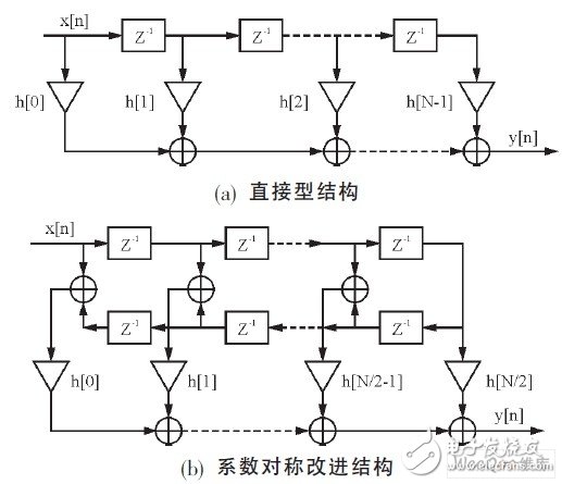
Figure 1 FIR filter structure
2 Design methods and indicatorsFDATool is a special filter design analysis tool in the Matlab signal processing toolbox. The main function of this tool is to extract filter coefficients according to design indicators. The key to designing digital filters with FDATool lies in the selection of parameters such as filter type, window function, filter order, and cutoff frequency. The window function is used to determine the stop band attenuation and transition band bandwidth. The commonly used window functions are rectangular window, Hanning window, Hamming window and Blackman window. Rectangular window and Hanning window have lower stop band attenuation, while Blackman window has a larger transition band. Relatively speaking, the Hamming window is more in line with the design requirements. Its minimum stop band can reach 54.5dB, and the normalized transition band bandwidth is 3.11Ï€/M (filter order N=2M+1). For sonic logging signals, the parameters listed in Table 1 should be set during design.
Table 1 Filter parameter selection
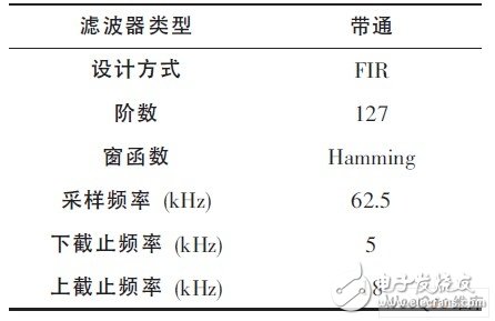
Figure 2 shows the amplitude-frequency and phase-frequency response curves of the filter. The curve maintains a linear phase in the passband, the stopband attenuation is greater than 52dB, and the transition bandwidth is 1.65kHz. The tap coefficients can be quantized as fixed-point integer data in the toolbox, so that a filter with an order of 127 can be implemented on the FPGA. The filter has a total of 128 coefficients. For a filter with a larger order, its quantization has minimal impact on the stop-band attenuation and transition band.

Figure 2 Filter amplitude frequency and phase frequency response characteristic curve
3 FPGA-based filter designThe key to designing FIR filters with FPGA is how to deal with multiplying units that take up a lot of resources. The proposed distributed algorithm (DA) can convert multiplication operations into shift-add operations, thereby saving hardware resources. If Hk is the filter coefficient, xk (n) is the sampling input at time n, and y (n) is the system response at time n, then equation (1) can be equivalent to the following equation:

The source data format of the data is specified as 2's complement form, then:

In the formula, xkb (n) is a binary number, which can be 0 or 1; xk0 (n) is the sign bit, 1 means the data is negative, and 0 means the data is positive. Therefore, substituting formula (4) into formula (3) can be obtained:

The form of equation (5) is called a distributed algorithm. It can be seen that the square brackets indicate that one data bit of the input variable and each bit of all filter tap coefficients H0 to HN are "ANDed" and summed. The exponent part explains the bit weight of the summation result. Multiplying an integer by 2b means shifting left by b bits. This can be achieved by hardware wiring without occupying logic resources. In this way, the operations in the square brackets can be realized by establishing a lookup table. The look-up table can be addressed by the same bit of all input variables. This is a distributed algorithm based on the look-up table (LUT-DA).
The size of the lookup table of the LUT-DA algorithm is B·2N bits, where B is the bit width of the input data, and N is the filter order. As the order of the filter increases, the size of the lookup table increases exponentially with 2; when B is 16 and N is 128, the size of the lookup table is unimaginable. Therefore, dividing the lookup table into multiple sub-tables can effectively solve this problem, which also derives more effective serial LUT-DA algorithms and parallel LUT-DA algorithms, but both have shortcomings. For the serial structure, to complete one output, multiple clock cycles greater than B are required; for the parallel structure, although one output can be completed in one clock cycle, it is necessary to copy B identical LUT tables, which will increase hardware resources s expenses.
In order to balance speed and area, this paper designs a CSD-DA algorithm based on the principle of DA algorithm. First, after expanding the fixed coefficient Hk in the coefficient equation (3) to the power of 2, we can get:
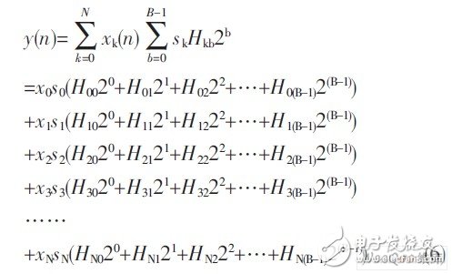
Then exchange the shift and accumulation order, then the following formula can be obtained:

In the formula, Hkb is a weight coefficient with a value of 0 or 1; Sk is 1 means Hk is positive, and -1 means Hk is negative; The value of s'kb can take 0, -1 or 1. After the expansion of formula (4), all multiplication operations will be converted to shift addition operations, where the part with a weight of 0 can be eliminated without calculation. In order to further reduce the non-zero entries in the Hkb array, Hk can be encoded as a CSD code, that is, starting from the least significant bit of the binary code, 10···01 is used to replace all 1 sequences greater than or equal to 2, and 1 means the The bit is -1. Since CSD indicates that any adjacent two bits must contain a 0, the number of 1s will not exceed N/2 at most. On average, CSD means that about 1/3 of the bits are non-zero, which is about 1/3 fewer non-zero bits than the complement. Suppose h= (15) 10= (01111) 2, y=hx=x (23+22+21+20), and if (15) 10 is encoded as (10001) csd, then Y=x· (24 -20). Using the binary encoding method, three adders will be used, while with CSD encoding, only one subtractor will be used. It can be seen that CSD encoding can substantially reduce hardware resource overhead. After CSD coding optimization, the number of non-zero values ​​of s'kb will be much smaller than the number of non-zero values ​​of Hkb.
For an FIR filter with symmetric linear phase coefficients, in order to reduce the multiplication unit, the structure shown in FIG. 3 may be selected. Since all multiplication operations can be converted into a large number of addition and subtraction operations, it will cause the critical path to be too long and the system to run at a slower speed. The addition of pipeline registers can reduce the length of the critical path, thereby increasing the maximum operating frequency of the system. When b is a fixed value, there is uncertainty in the number of non-zero values ​​of s′kb. Therefore, during pipeline design, flexible segmentation can be performed according to s′kb. The longer the path, the more pipeline registers are added. In order to prevent the overflow of intermediate results, the bit width of the register should be designed redundantly. For signed numbers, the bit width is M+log2N-1, M is the bit width of the upper accumulator, and N is the filter order.
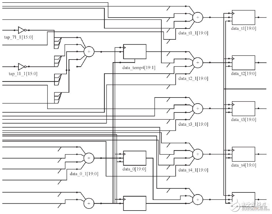
Figure 3 The local structure of the pipeline CSD-DA algorithm
It can be seen from the pipeline optimization CSD-DA algorithm structure in Figure 3 that all multiplications will be converted to shift addition, and the shift operation can be implemented by hardware connections, and the entire structure has undergone a reasonable pipeline segmentation.
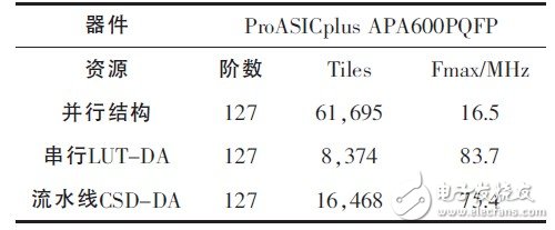
Table 2 lists the comprehensive results of filters with different structures. Among them, the parallel structure is the worst structure, which occupies a lot of resources and is slow; the serial LUT-DA structure, although it occupies less resources and has a high maximum operating frequency, is a serial structure after all, and it cannot be done in one clock tick. One sampling point filtering operation; while the pipeline CSD-DA structure has obvious advantages in terms of speed and area. If the working clock is 75MHz, then one clock tick can complete one output, and it only takes 4.4μs to process a single channel signal of 330 sampling points, which can meet the real-time logging requirements.
Table 2 Comprehensive results of the filter
In order to verify whether the function of the filter is correct, the design can be simulated in Modelsim. If the original waveform is an acoustic signal with noise, then the filtering result is shown in Figure 4.
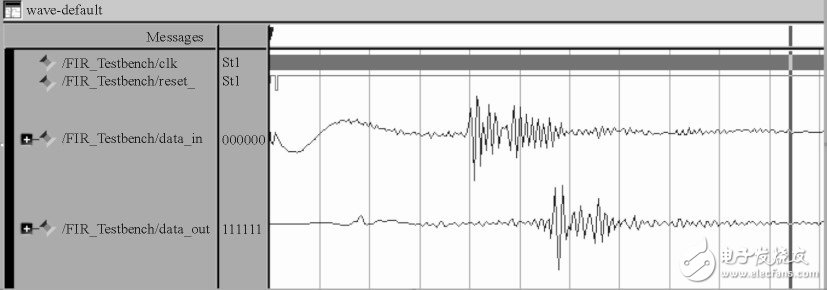
Figure 4 Simulation results of the filter in Modelsim
Figure 5 shows the simulation results of the filter in Matlab. It can be seen that the simulation results of Modelsim and Matlab are consistent. In the frequency domain, comparing Figure 5 (a) and Figure 5 (b), it can be seen that the filtered waveform only retains the frequency spectrum part of 5kHz~18kHz, which shows that the digital filter of the pipeline CSD-DA structure is designed correctly.
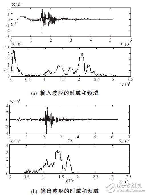
Figure 5 Simulation results of the filter in Matlab
5 concluding remarksThis article describes in detail the method of designing FIR linear phase filters through Matlab tools, and designs a pipelined CSD-DA structure that is superior to the traditional structure for acoustic signals. This structure has obvious advantages in speed and area. The paper also verified the rationality and correctness of the design through simulation experiments. But it is worth pointing out that this structure is only suitable for the occasion of fixed filter coefficients, and if it is to be modified, the coefficients need to be CSD coded and pipelined again.
Photovoltaic Power Generation Equipment
Photovoltaic Power Generation Equipment,Photovoltaic Power Generation,Solar Photovoltaic Power Generation,Wind Power And Photovoltaic Power Generation
TRANCHART Electrical and Machinery Co.,LTD , https://www.tranchart-electrical.com