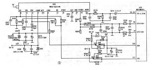
First, the RF signal input circuit analyzes and repairs the single chip MST6M69FL (U39) used in this machine, supports 8 analog input ports, and can directly decode analog composite video and S-VIDEO video. The LT42710FHD model uses an integrated tuner, and the tuner circuit is shown in Figure 1. The pin function of the integrated tuner U30 (TMI8-C2211VH) is shown in Table 1.
1, signal processing circuit
The RF analog TV signal enters the tuner U30, is internally demodulated, mixed into an IF signal, and then enters the IF amplifier IC. After intermediate frequency amplification and demodulation, the CVBS video signal is output from the U30 (12) pin, first through R402 and R394. Partially divided, R173, L69 are coupled, and then R192, C59 and R195, C60 form a differential signal, which is sent to the (46) and (47) pins of the main chip U39. Differential signal input enhances signal stability. At the same time, the audio signal demodulated by U30 is sent to the (58) and (59) pins of U39. If the U30 (12) pin has no normal video signal output (the oscilloscope can measure the video signal waveform, it can also measure the DC voltage to make a preliminary judgment: 0.8V when there is a signal; 1.2V when there is no signal), you need to check the external components first.
2. Tuning voltage forming circuit The tuning voltage forming circuit is composed of elements such as D70 (BAS62-A13), D72 (BAS62-A13), and D74 (μPC574). Regulator U45 (LM2596-ADI) 2-pin output frequency 150kHz, amplitude 24V square wave pulse, sent to the voltage doubler rectifier circuit, and then output a stable +33V voltage to the U30's 3 feet, for the high frequency head A stable 33V tuning voltage for use with the varactor diodes inside the tuner.
Second, AV signal input circuit analysis
1.AV2 input circuit
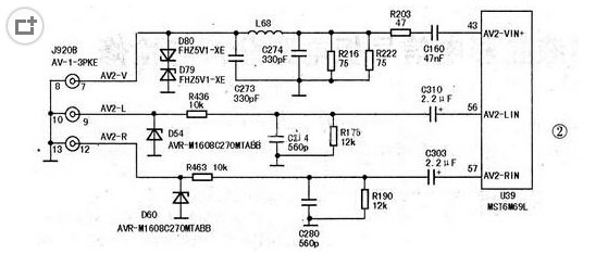
The AV2 video signal is input from the AV socket J920B, and is coupled to the (43) pin of the U39 via L68, R216, R203, and C160, as shown in FIG. Diodes D80 and D79 provide protection. The AV2 audio signal (AV2-Lin) is input from the AV socket J920B, and is low-pass filtered by D54, R438, C284, and R176 (after suppression of the interference signal) to enter the U39 (56) pin. Diode D54 serves as a protection. The AV2 audio signal (AV2-Rin) is input from the AV socket J920B, and is low-pass filtered by D60, R463, C280, and R190 to enter the U39 (57) pin. Diode D60 acts as a protection.
2.AV1 input circuit
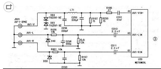
The AV1 video signal is input from the side AV jack J921 and coupled to the U39 (44) pin via the inductor L71, the resistor R186 and the capacitor 0, 161, as shown in FIG. D84, D83 are protection diodes to prevent the input signal amplitude from being too high or electrostatic damage. U39.AV1 audio signal (AVl-Lin) is input from AV socket J921, low-pass filtered by D48, R436, C298, R189, and then coupled via capacitor C310 To the U39 (60) foot. The AV1 audio signal (AVl-Rin) is input from the AV socket 1921, low-pass filtered by R461, R197, C193, and then coupled to the U39 (61) pin via the capacitor C311.
Third, S terminal signal input circuit analysis
1, the back S terminal circuit
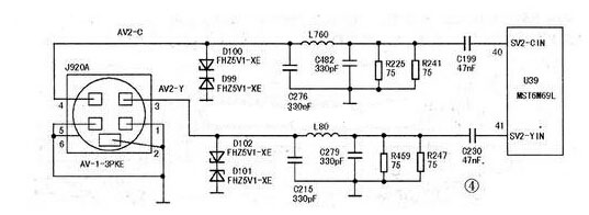
The AV2-Y luminance signal is coupled to the U39 (41) pin via the inductor L80 and the capacitor C230, and the resistors R459 and R427 are the reference grounding resistor of the U39 (41) pin. The AV2-C chrominance signal is coupled to the (40) leg via L76 and C199.
2. Side S terminal circuit
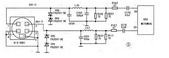
The AVl-Y luminance signal is coupled to the U39 (39) pin via L67, R167, C175, as shown in FIG. D95 and D94 are protection diodes. The AVl-C chrominance signal is coupled to the U39 (38) pin via L70, R164, C176. D98 and D96 are protection diodes.
Fourth, YPbPr interface input circuit analysis component Y signal is divided into two channels after the inductor L49, as shown in Figure 6, one path is isolated by resistor R125, C158 is coupled to U39 (30) pin; the other is isolated by resistor R126, capacitor C159 is coupled To the U39 (31) pin, as the Y sync signal. D45 and D43 are protection diodes. The U39 (29) pin is the Y-signal input of the differential signal, and the external resistor R133 and capacitor C56.
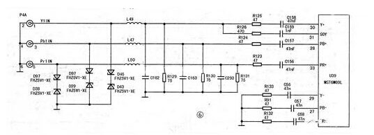
The Pb signal is coupled to the U39 (28) pin via L47, R124, C157, and the (27) pin is the Pb-signal input, with external resistor R91 and capacitor C57. The Pr signal is coupled to the U39 (33) pin via L50, R123, C156, the (32) pin is the Pr signal reference voltage ground potential, and the external resistor R132 and capacitor C58. If the U39 does not detect the normal Y-synchronization signal of the (31) pin, high-definition no-picture phenomenon will occur; if the input color difference signal Pb or Pr is abnormal, the color signal of the high-definition signal will be abnormal.
Five, VGA interface input circuit analysis
The VGA primary color signal enters through the connectors P31~3, and is then isolated by resistors R95~R97. The capacitors C147, C134, and C142 are coupled to U39(26), (25), and (23) pins, as shown in Figure 7. The bidirectional limiting diodes D24~D26 provide protection against abnormal damage to the manifold due to static electricity or input voltage. The G primary color signal input through the connector P32 pin is also isolated by R98, and the capacitor C136 is coupled to the U39 (24) pin for use as a synchronization signal.
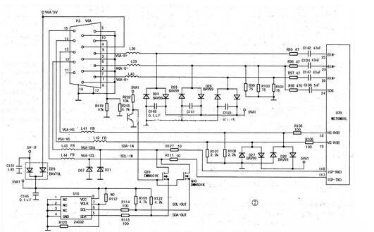
The line and field sync signals are input from the (13) and (14) pins of the connector P3, and sent to the U39 (8) and (19) pins via the inductors L41 and L42 and the resistors R105 and R106. The bidirectional limiting diodes D27 and D28 provide protection. The memory U16 (24C02 ($0.2400)) stores the "identity" data of the TV recognizable by the PC in accordance with the VGA format requirement. The P3(12) and (15) pins are connected to the 5th and 6th pins of the memory U16. The P34 pin external transistor Q24 controls the on/off of the SCL and SDA lines input to U16. When the PC is turned on, the control signal turns on Q24, the FET Q39.Q40 turns on, and the PC bus is connected to the 5 and 6 pins of U16 to complete mutual communication. If the line, field sync signal input by the VGA interface, or the G sync signal input by the DDR channel and U39 (24) pin is abnormal, it will cause a VGA no picture fault; if the input primary color signal is not normal, it will result in a VGA image. The color is not normal.
Sixth, HDMI interface input circuit analysis
The HDMI interface circuit is mainly composed of HDMI switch PS321 ($2.1420), protection circuits U20, U32 and U34, U35, memory U14, U15, etc., as shown in FIG. This unit has two HDMI receiving ports and is also compatible with DVI/HDCP receiving standards. HDMI-1 is divided into two channels after input through the interfaces Pl7/9, 4/6, 1/3, (10)/(12), and sent to U32 and U20 for protection. The other is sent to U5 ( 5/6, 8/9, (11)/(12)), (14)/(15) feet of PS321). The bus data signal sent from the (15) and (16) pins of the HDMI-1 interface P1 is connected to the 5th and 6th pins of the U14 (M24C02 ($0.0853)), and the TV hardware parameter information is read therefrom for the HDMI to the TV. The machine is identified and communicated with the 2 and 3 pins of U5 (PS321).
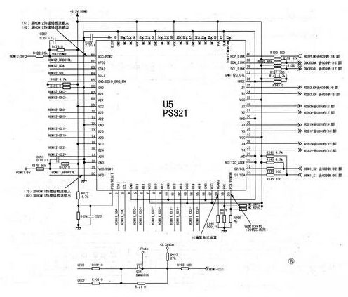
When HDMI-1 is turned on, the +5V voltage is sent from the HDMI-1 interface P3 (18), which provides the working voltage for U14 (M24C02). On the other hand, it provides the bias for the hot-plug control transistor Q8 after R78. Set the voltage.
When using the remote control or the local button to switch to the HDMI-1 state, the (14) pin of U39 outputs the hot-plug identification signal to the (40) pin of U5, and the HDMI-1 is output from the (80) pin after U5 internal switching. The interface hot plugs the identification signal (low level), Q8 is cut off, and its c-pole output is high level, and is sent to the HDMI-1 output device via the P3 pin 10 as the identification signal. After the output device detects the normal hot-plug signal, it starts to read the E-EDID data stored by U14 (M24C02) through the bus. After reading the normal, it reads from U29 (M24C04 ($0.0714)) through the I2C bus. Take decryption information and exchange passwords. If it is in non-HDMI state, U5 (80) pin outputs HDMI-1 interface hot plugging identification signal (+5V high level), Q8 saturates on, HDMI-1 output device detects P3 (19) pin low level After the stop signal output. LCD TVs must display the information of the received HDMI-1 interface normally, and require low-voltage differential signals (including audio and video signals, clock signals and other auxiliary signals), hot-plug signals, DDC channels, and U509 and U501 input to the switching chip. The data is normal.
Seven, USB interface input circuit analysis
U31 (FSUSB30MUX ($0.6120)) is a low power dual channel Hi-Speed ​​USB 2.0 switch. As shown in Figure 9, the signal input from the USB1 interface is sent to pins 2 and 8 of U31, and the signal input from the USB2 interface is sent to pins 3 and 7 of U31. Under the control of the 1-pin selection signal of U31, it outputs from the 4th and 6th pins of U31 to the (249) and (250) pins of U39; when the 1st pin of U31 is high, the USB2 input is selected; when the 1st pin is low At the level, select the USB1 input.
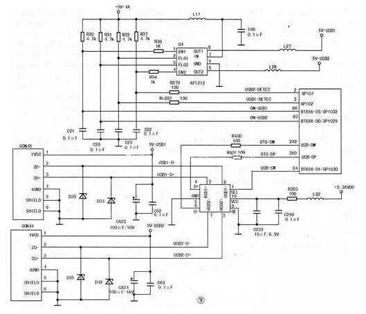
U4 (AP1212HSL -13) is a dual USB power management IC that controls the independent output of two power supplies through high and low level on/off signals, and has overcurrent protection function. When the USB external device fails and the output current exceeds 1A, 1C will automatically cut off the power output and generate a fault indication signal. When using the remote control or the local button to switch to the USB1 state, the (26) pin of U39 outputs a high level to the 1 pin of U4, and the 5V-USB1 voltage is output from the 8 pin to the CON45 socket. When using the remote control or the local button to switch to the USB2 state, the (83) pin of U39 outputs a high level to the 4 pin of U4, and the 5V-USB1 voltage is output from the 5 pin to the CON44 socket.

The 60W Macbook Charger with MagSafe1 or Magsafe 2 Power Adapter has a magnetic DC connector, so if someone trips on it, the power cord disconnects harmlessly, keeping your MacBook Air safe. It also helps prevent the cable from fraying or weakening over time. Additionally, the magnetic DC helps guide the plug into the system for a quick and safe connection.
60W Apple charger usb c,60w charger macbook air,macbook 60w charger
Shenzhen Waweis Technology Co., Ltd. , https://www.szwaweischarger.com