The common reset design methods used in FPGA design are classified, analyzed and compared. In view of the phenomenon of unreliable reset in the reset process of FPGA, four methods to improve the reliability of reset design are proposed, including clearing the glitch on the reset signal, asynchronous reset synchronous release, using dedicated global asynchronous reset/set resource and adopting internal Reset. The above method can effectively improve the reliability of the FPGA reset.
For the FPGA chip, before the power is applied to the chip, the changes of the potentials of the various nodes inside the chip are uncertain and uncontrollable, and this uncertain and uncontrollable situation will cause the chip to work after power-on. error. Therefore, in the design of the FPGA, in order to ensure that the system can enter the working state reliably, and to avoid adverse effects on the system associated with the FPGA output, the FPGA should be reset after power-on, and in order to eliminate the jitter caused by the power switch process, The reset signal needs to be cancelled after a certain delay after the power supply is stable. The reset signal of the FPGA must be correct, stable and reliable.
In the design of the FPGA, in most cases, the function of the reset circuit can be completed normally, but the circuit is not accurately and reasonably designed, and there are still reliability design defects. In order to ensure the reliability of the system reset, it is necessary to study the reliability design method of FPGA reset.
1 reset design method classification
The purpose of the reset is to force the design to be in a known state during simulation. Reasonable selection of the reset mode is the key to circuit design. According to the relationship with the system clock domain, the reset circuit can be divided into synchronous reset and asynchronous reset. Synchronous reset means that the reset signal is valid only when the clock edge comes. Otherwise, the reset of the system cannot be completed. Asynchronous reset means that the system is reset as long as the clock edge is coming, as long as the reset signal is valid.
The reset circuit can be further divided into an external reset and an internal reset depending on whether an external reset port is present. External reset means that the reset signal is mainly from the input of an external pin, such as the reset button, power module output, and so on. The internal reset signal is generated primarily by the internal circuitry of the FPGA.
2 comparison of design methods
2.1 synchronous reset and asynchronous reset
2.2.1 Synchronous reset
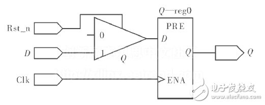
When a synchronous reset is specified, there is only one clock edge signal in the always sensitive table. Only when the clock edge acquires the active level of the synchronous reset, will the reset operation be performed at the arrival of the clock edge. If the trigger in the target device or the available library itself contains a synchronous reset port, the synchronous reset terminal can be called directly when implementing the synchronous reset circuit. However, most of the target device's flip-flops do not include a synchronous reset port. The reset signal and the input signal form a combinational logic and then input to the input of the register. In order to increase the priority of the reset circuit, the if...else structure with priority is usually used in the circuit description. The reset circuit is described under the first if, and the other circuits are described in the else or else...if branch. The RTL diagram after the reset circuit is integrated is shown in Figure 1.

Figure 1 synchronous reset circuit diagram
Support Plate Shaft,Shaft Support Plate,Shaft Supports,Bearing Support Plate
Changzhou Youeryou Trading Co., Ltd. , https://www.farmpartssupplier.com