The skill of designing efficient and compact DC/DC converters is carried out by a group of engineers who have a deep understanding of the physics and supporting mathematics involved in conversion design and have a certain level of bench experience. A deep understanding of Bode diagrams, Maxwell's equations, and attention to poles and zeros are incorporated into the sophisticated DC/DC converter design. However, IC designers often steer clear of the worrying heat issues that often lie on the packaging engineer.
For point-of-load (POL) converters, heat is a big problem. These converters are compact and accommodate many ICs that need to be treated with care. The reason why POL regulators generate heat is because there is no voltage conversion efficiency of 100%. How much structure, layout, and thermal resistance can the package heat up? The thermal resistance of the package not only increases the temperature of the POL regulator, but also increases the temperature of the PCB and surrounding components, thus increasing the complexity of the system's thermal solution. , size and cost.
There are two main ways to reduce the heat of the DC/DC converter package on the PCB:
Heat dissipation through the PCB: If the converter IC is surface mountable, the copper vias and copper foil that conduct heat in the PCB can dissipate heat from the bottom of the package. If the thermal resistance of the package to the PCB is low enough, then this method can be used to dissipate heat.
Increased air flow: A cold air stream can dissipate heat from the package (or more accurately, heat is transferred to air molecules that are in contact with the package surface and that are cooler and move faster).
Of course, there are passive and active cooling methods. For the sake of simplicity, we have classified both passive and active cooling methods as a subset of the second method described above.
When faced with component temperature rise, PCB designers can look for common methods in some standard cooling methods: use more copper, heat sinks or larger, faster fans, or just more space - increase PCB The distance between the space and the components on the PCB or the thickened PCB layer.
Either of these methods can be used to keep the system within safe temperature limits on the PCB, but using these methods may reduce the market competitive advantage of the final product. The final product (such as a router) may therefore require a larger enclosure to allow for the necessary component separation on the PCB, or perhaps a relatively large noise due to the addition of a faster fan to enhance air flow. In a market where companies compete in terms of compactness, computing power, data transfer rate, efficiency and cost advantages, this may make the final product look poor.
Achieving successful thermal management around a high-power POL regulator requires the selection of an appropriate voltage regulator, which requires careful investigation. This article shows how to choose a voltage regulator to simplify the work of the board designer.
Don't rely solely on power density to judge POL regulatorsSeveral market factors have led to the need to improve the thermal performance of electronic devices. The most obvious is that even if the product size is shrinking, the performance is constantly improving. For example, digital devices from 28nm to 20nm and below 20nm consume more power to improve performance because designers of innovative devices use faster, more compact, less noisy, and more efficient technology with smaller process technologies. Device. From this trend it is clear that the POL regulator must increase the power density: (power) / (volume) or (power) / (area).
In the literature on regulators, power density often appears in the headings of performance specifications, which is not surprising. The excellent power density makes the regulator stand out. When designers choose among a large number of available voltage regulators, such power density becomes a quotable specification. A 40W/cm2 regulator must be better than a 30W/cm2 regulator.
If product designers want to provide more power in a more crowded space, excellent power density numbers will first come to mind and become the clearest way to achieve the fastest, smallest, quietest, and most efficient products, just like horsepower. Compare car performance. But how important is power density in achieving a successful final design? The importance is lower than expected.
A POL regulator must meet the needs of its application. When choosing a POL regulator, you must ensure that it can perform tasks on the PCB. On the PCB, thermal processing may or may not ruin the application. The following recommended step-by-step selection of POL regulators prioritizes thermal performance:
Ignoring power density figures: Power density specifications ignore the thermal derating problem, and thermal derating has a considerable impact on effective, true “power densityâ€.
Look at the thermal derating curve of the regulator: A detailed, well-characterized POL regulator should have some graphs that specify the output current at different input voltages, output voltages, and gas flow rates. The data sheet should show the output current capability of the POL regulator under real operating conditions to determine if the regulator is suitable for its thermal performance and load current capability. Does it meet the typical and maximum ambient temperature and airflow requirements of the system? Remember that the output current derating is related to the thermal performance of the device. These two points are closely related and equally important.
Consider efficiency issues: Yes, efficiency is not the first issue to consider. When considered separately, the efficiency value may not represent the exact DC/DC regulator thermal characteristics. Of course, efficiency figures are needed when calculating input current and load current, input power consumption, power consumption, and junction temperature. However, the efficiency value must be considered in conjunction with the output current derating and other thermal data associated with the device and its package.
For example, a 98% efficiency DC/DC buck converter is impressive; it is even more impressive when the converter has excellent power density figures. Would you buy such a regulator instead of a less efficient, lower power regulator? A practical engineer would ask for the seemingly unimportant 2% loss of efficiency. How does the lost power translate into a rise in package temperature during operation? What is the junction temperature of a high power density, high efficiency regulator at 60 ° C ambient temperature, 200 LFM flow? Look at the room temperature beyond the listed 25 ° C A situation other than the typical number below. What is the maximum and minimum measured at extreme temperatures of −40°C, 85°C, or 125°C? At high power densities, the thermal resistance of the package rises so high that the junction temperature rises sharply beyond safety. Is the operating temperature? How much does an impressive but expensive regulator need to be derated? Does the derated output current limit the output power capability so that the high price of the device is no longer reasonable?
Consider whether the POL regulator is easy to cool: The thermal resistance of the package provided in the data sheet is the key to simulating and calculating the junction temperature of the device, the ambient temperature, and the rise in case temperature. Because most of the heat in a surface mount package flows from the bottom of the package to the PCB, a clear layout guide must be given in the data sheet and questions about thermal measurements should be explored to minimize accidents when generating system prototypes.
A well-designed package should dissipate heat evenly and efficiently through its surface, eliminating hot spots that can degrade the reliability of the POL regulator. As mentioned above, the PCB is responsible for absorbing and delivering most of the heat from the surface mount POL regulator. However, in today's complex systems with densely packed components, forced air flow is commonly used. A well-designed POL regulator should also take advantage of this “free†cooling opportunity to eliminate the heat generated by heat-generating components such as MOSFETs and inductors. .
Direct heat to the top of the package and into the airThe high power switching POL regulator relies on an inductor or transformer to convert the input supply voltage to a stable output voltage. In a non-isolated buck POL regulator, the device uses an inductor. The accompanying switching components, such as inductors and MOSFETs, generate heat during DC/DC conversion.
About a decade ago, a new packaging technology advancement allowed the entire DC/DC regulator circuit, including magnetic components, to be designed into a molded plastic package called a module or SiP, molded plastic package interior. Most of the heat generated is sent to the PCB through the bottom of the package. Any conventional method that improves the heat dissipation capability of the package can result in an increase in the package, such as attaching a heat sink to the top of the surface mount package.
A few years ago, an innovative module packaging method was developed that used the available airflow to help cool. This package design integrates a heat sink into the module package and is fully molded. Inside the package, the bottom of the heatsink is connected directly to the heat-generating MOSFET and inductor, while the top of the heatsink is a flat surface exposed on top of the package. This new in-package cooling method allows the device to cool quickly with airflow (for example, watch the LTM4620 Technical Video clip).
Vertical structure: POL module regulator with stacked inductors as heat sinkThe size of the inductor in a POL regulator depends on the voltage, the switching frequency, the current to be processed, and its structure. In the modular approach, the DC/DC circuit, including the inductor, is completely molded and sealed in a plastic package, just like an IC, compared to any other component, the thickness and volume of the package to the package. The weight is more decisive. Inductors are also an important source of heat.
The above method of integrating the heat sink into the package helps to transfer the heat from the MOSFET and inductor to the top of the package, which can then dissipate heat into the air, cooling plate or passive heat sink. This method is effective when a relatively small, low-current inductor is easily incorporated into a plastic molded package, but this method is less effective when a POL regulator uses a larger, larger current inductor. At this point, placing magnetic components inside the package forces other circuit components to be further separated, significantly increasing the footprint of the package on the PCB. In order to maintain a small footprint and improve heat dissipation, package engineers have developed another clever approach: vertical, stacked or 3D (Figure 1) structures.
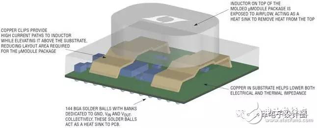
Figure 1: The high-power POL regulator module uses a 3D (vertical) package technology to raise the inductor and expose the inductor to airflow as a heat sink. The DC/DC circuit is mounted on the substrate under the inductor, thus minimizing the PCB footprint required while improving thermal performance.
3D package with exposed stacked inductors: maintains small footprint, increases power and improves heat dissipationWith a small PCB footprint, greater power and better thermal performance, these three advantages can be achieved in a 3D package, a new POL regulator construction method (Figure 1). The LTM4636 is a μModule regulator with built-in DC/DC regulator ICs, MOSFETs, supporting circuitry and a large inductor to reduce output ripple and provide a precision from 3.3V to 0.6V from a 12V input. 40A load current. Four LTM4636 devices operating in parallel share the current to provide 160A of load current. The footprint of the package is only 16mm x 16mm. Another regulator in the series, the LTM4636-1, detects overheating and input/output overvoltage conditions and can disconnect the upstream power supply or circuit breaker to protect itself and its load.
Horsepower advocates can calculate the power density of the LTM4636, and the resulting numbers can be safely advertised as impressive, but as noted above, the power density figures do not tell the full story. This μModule regulator also brings other important benefits to system designers: the impressive thermal performance of the DC/DC converter efficiency and unmatched heat dissipation.
To minimize the regulator footprint (16mm x 16mm BGA), the inductor is raised and attached to two copper leadframe structures for other circuit components (diodes, resistors, MOSFETs, The capacitor, DC/DC IC) can be soldered to the substrate under the inductor. If the inductor is placed on a substrate, the μModule regulator can easily occupy more than 1225mm2 of PCB area instead of 256mm2 of board area (Figure 2).
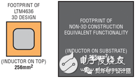
Figure 2: The stacked inductor of the LTM4636 acts as a heat sink at the same time. As a complete POL solution, the device achieves impressive thermal performance with a small footprint.
The stacked inductor structure provides system designers with a compact POL regulator with additional thermal performance advantages. The stacked inductors in the LTM4636 are not fully molded (sealed) with plastic like the rest of the components. Instead, the inductor is directly exposed to the airflow. The inductor housing is rounded to improve aerodynamics (to achieve minimum flow resistance).
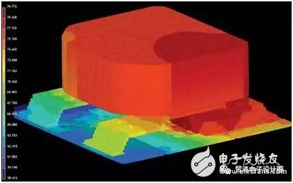
Figure 3: The thermal performance of the LTM4636 molded micromodule shows that heat is easily transferred to an inductor package that is exposed to airflow.
Thermal performance and efficiencyThe LTM4636 is a 40A μModule regulator that benefits from 3D packaging technology or component-level packaging (CoP), as shown in Figure 1. The package is a fully molded 16mm x 16mm x 1.91mm BGA package. The LTM4636's inductors are stacked on top of the molded package, with a total package height of 7.16mm from BGA solder balls (144 total) to the top of the inductor.
In addition to heat dissipation from the top, the LTM4636 is designed to efficiently dissipate heat from the bottom of the package to the PCB. The device has 144 BGA solder balls in a row dedicated to GND, VIN, and VOUT through which large currents flow. These solder balls are combined to provide heat dissipation to the PCB. The LTM4636 is optimized for heat dissipation from the top and bottom of the package.
Even with such a large conversion ratio of 12V input / 1V output and 40A (40W) full load current and standard 200LFM airflow, the LTM4636 package temperature only rises above ambient temperature (25°C to 26.5°C) 40 ° C. Figure 4 shows the thermal image of the LTM4636 under these conditions.
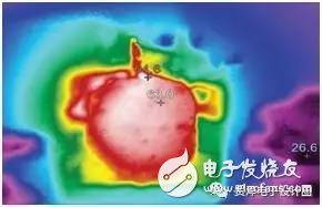
Figure 4: Thermal image of the regulator at 40W, temperature rises only 40°C
Figure 5 shows the output current thermal derating results. At 200LFM, the LTM4636 delivers an impressive 40A full current at ambient temperatures up to 83°C. The 20A half current derating only occurs at excessive ambient temperatures of 110 °C. This allows the LTM4636 to operate at high capacity as long as a certain airflow is available.
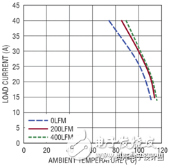
Figure 5: Thermal derating graph showing 40A full current at ambient temperatures up to 83°C and 200LFM
The high conversion efficiency shown in Figure 6 is primarily due to the high performance MOSFET and the powerful LTM4636 driver. For example, a 12V input power step-down DC/DC controller:
95% efficiency at 12V input to 3.3V, 25A output
93% efficiency at 12V input to 1.8V, 40A output
88% efficiency at 12V input to 1V, 40A output
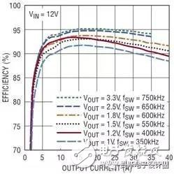
Figure 6: High DC/DC conversion efficiency at various output voltages
Thermally balanced 140W, expandable 4 x 40A μModule POL regulatorOne LTM4636 is specified to provide 40A load current. Two LTM4636s with current sharing mode (or parallel) support 80A current, while four parallel LTM4636s support 160A current. Extending the power supply with the parallel LTM4636 is easy: simply copy and paste a single regulator layout as shown in Figure 7 (symbols and layouts available).
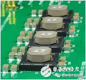
Figure 7: It is easy to place the parallel LTM4636. Simply copy the single channel layout.
The LTM4636's current mode architecture achieves accurate current sharing between 40A components. Accurate current sharing in turn produces a power source that evenly dissipates heat between devices. Figure 8 shows that in a 160A regulator consisting of four μModules, all devices operate within 1°C of each other, ensuring that each device is not overloaded or overheated. This greatly simplifies heat dissipation.
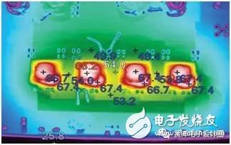
Figure 8: Accurately divide the current between the four LTM4636s operating in parallel, with a temperature rise of only 40°C for 160A applications.
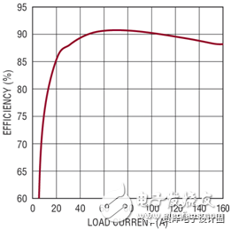
Figure 9: Efficiency of four μModule regulators providing 140W power
Figure 10 shows the complete 160A design. Note that the LTM4636 operates differently from each other without the need for a clock device, and clock and phase control are included in the device. Multiphase operation reduces output and input ripple current, reducing the number of input and output capacitors required. The four LTM4636s in Figure 10 operate with a 90° phase difference.
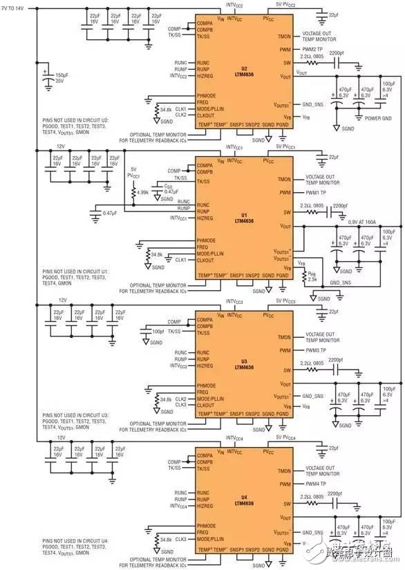
Figure 10: The 140W regulator consists of four LTM4636s running in parallel, providing accurate current sharing and high efficiency conversion from 12V input to 0.9V, 160A output.
in conclusionChoosing a POL regulator for a densely packed system requires a rigorous review of specifications other than the device voltage and current ratings. Evaluation of the thermal characteristics of the package is essential because it determines the cost of cooling, the cost of the PCB, and the size of the final product. Advances in 3D (also known as overlay, vertical, CoP) technology allow high-power POL modular regulators to take up very little PCB area, but more importantly, achieve high efficiency cooling. The LTM4636 is the first device in the μModule family of regulators to benefit from this stacked package technology. As a 40A POL μModule regulator with a stacked inductor as a heat sink, the device delivers 95% to 88% efficiency, with a temperature rise of only 40°C at full load, consuming 16mm x 16mm PCB area. A video introduction to the LTM4636 is available on the LTM4636.
This article is reproduced from Linear Technology
Disclaimer: This article is a reprinted article. The purpose of reprinting this article is to pass on more information. The copyright belongs to the original author. If it involves infringement, please contact Xiaobian for processing.
About the Moser Electronic Design CircleThe Moser Electronics Design Circle is developed and operated by Mouser Electronics to serve the global electronics design community. The company distributes more than 600 leading brands and can order more than 4 million online products for design engineers and procurement personnel. Provide one-stop shopping platform, welcome to pay attention to us, get first-hand design and industry information!
China leading manufacturers and suppliers of DC Support Capacitors,DC Capacitor, and we are specialize in Electrolytic capacitor,High Voltage Capacitor, etc.DCMJ DC Support Capacitors
DCMJ DC Support Capacitors,Capacitors High Voltage,Dc-link Filter Capacitor,Dc Film Capacitors
YANGZHOU POSITIONING TECH CO., LTD. , https://www.pst-thyristor.com