This paper is mainly for double-tube RC-coupled amplifier and circuit fault analysis.
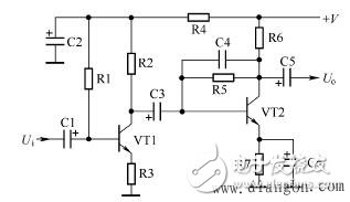
Figure 1 shows a dual-tube RC-coupled amplifier. This multistage amplifier consists of two single-stage amplifiers, which are capacitively coupled between them, so they are called dual-tube RC-coupled amplifiers.

Figure 1 Double-tube RC-coupled amplifier
1. Single-stage amplifier type identification method and analysis and understanding of working principle of DC and AC circuits
In this multistage amplifier, two transistors VT1 and VT2 form a two-stage amplifier, and two single-stage amplifiers are coupled by a capacitor C3. In the circuit, VT1 is the first stage amplification tube, VT2 is the second stage amplification tube, Ui is the input signal, and Uo is the output signal amplified by the two stage amplifier.
1. First stage amplifier type identification
It can be seen from the circuit that the input signal is input from the base of the transistor VT1, and the amplified signal is output from its collector, so this is a first-level common emitter amplifier.
2. Second stage amplifier type identification
The signal output from the first stage amplifier is input from the base to VT2 via the coupling capacitor C3, and the amplified signal is output from its collector. This is also a Class 1 common emitter amplifier, so this is a cascode-common dual amplifier.
3. DC circuit analysis
This multi-stage amplifier uses the capacitor C3 for interstage coupling, so the DC circuits of the two-stage amplifier are separately analyzed. The analysis of the DC circuit of this double-tube RC-coupled amplifier mainly explains the following points:
(1) DC operating voltage + V is applied to the VT2 collector via R6, + V is applied to the VT2 base via resistors R6 and R5, and R7 grounds the VT2 emitter.
(2) DC operating voltage + V is decoupled and filtered by R4 and C2 and applied to the first stage amplifier to provide DC operating voltage.
(3) R2 is the VT1 collector load resistor, which provides DC operating voltage for VT1. R1 is the VT1 fixed bias resistor and R3 is the VT1 emitter negative feedback resistor.
4. AC circuit analysis
The AC input signal Ui is coupled to the base of VT1 via the input coupling capacitor C1, double-amplified by VT1 voltage and current, and output from its collector. It is applied to the base of VT2 through the interstage coupling capacitor C3, and is amplified by VT2 voltage and current. It is then output from its collector and applied to the post-amplifier via the output coupling capacitor C4.
The working principle of the AC circuit of this double-tube RC-coupled amplifier also explains the following points:
(1) From the perspective of signal voltage, the signal voltage on the VT1 collector is greater than the signal voltage on the base. The signal voltage on the VT2 collector is greater than the signal voltage on the base. The signal voltage in VT2 is greater than VT1. Signal voltage in .
(2) Since this is a cascode-common dual-tube amplifier, the common-emitter amplifier of each stage shifts the signal voltage by 180°, and the two-stage amplifier shifts phase by 360°, so the output signal voltage Uo phase and input signal voltage Ui has the same phase.
(3) The signal transmission process of this double-tube amplifier is: AC input signal Ui → C1 (coupling) → VT1 base → VT1 collector → C3 (inter-stage coupling) → VT2 base → VT2 collector → C5 → output signal The voltage Uo is in the circuit of the latter stage.
2, component role analysis and circuit failure analysis
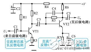
In order to analyze the circuit, the circuit is redrawn into the circuit shown in Figure 2.

Figure 2 Double-tube RC-coupled amplifier
1. Analysis of the role of components
VT1 and VT2 use different base bias circuits. VT1 uses a fixed bias circuit, and VT2 uses a collector-base negative feedback bias circuit.
There is no shunt bypass capacitor on the VT1 emitter resistor R3, so R3 has negative feedback for both AC and DC.
R4 is the DC voltage supply resistor of the first stage amplifier and also the decoupling resistor in the multistage amplifier. The decoupling effect on it will be described in detail in the decoupling circuit. From the perspective of the DC circuit, the DC operating voltage applied to the first stage amplifier is reduced by R4 because the DC current generated by the DC operating voltage + V passes through R4 and there is a voltage drop across R4, which makes the DC of the first stage amplifier The operating voltage is lower than the DC operating voltage of the second stage amplifier.
C2 is the filter and decoupling capacitor. If C2 is not connected, resistor R4 will be part of the VT1 collector load resistor (R4 and R2 are connected in series as the VT1 collector load resistor). After accessing C2, the VT1 collector AC signal current does not flow through R4 (flow through R2 AC current through C2 to the ground), only through R2, so only R2 is the VT1 collector load resistance.
2. Circuit failure analysis
The fault analysis of this dual-tube RC-coupled amplifier is basically the same as that of a single-stage amplifier. The differences are as follows:
(1) When the DC circuit in the VT1 amplifier fails, the DC circuit of the VT2 amplifier will not be affected due to the DC blocking function of C3. Since the first stage amplifier is no longer functioning properly, it does not have a normal output signal applied to the second stage amplifier. Although the second stage amplifier can work normally, the entire double tube amplifier has no signal output.
(2) After the failure of the DC circuit of the second stage amplifier, since the presence of C3 does not affect the operation of the DC circuit of the first stage amplifier, the first stage amplifier can output a normal signal. Since the second stage amplifier does not work properly, the second stage amplifier cannot output a normal signal. It can be seen that as long as there is a problem with the primary amplifier in the multi-stage amplifier, the entire multi-stage amplifier cannot output a normal signal.
(3) When C2 is open, there is no effect on the second stage amplifier, which will increase the voltage of the output signal of the first stage amplifier because the load resistance of the VT1 collector is increased by R4. When C2 leaks or breaks down, the DC operating voltage of the first stage amplifier becomes smaller or no DC voltage, and the current flowing through R4 increases, which also causes the DC operating voltage + V to decrease and affect the normal operation of the second stage amplifier. At this time, the entire amplifier has no output signal or the signal is small.
Circuit analysis summary
(4) When the resistor R4 is open, the first stage amplifier has no DC operating voltage and does not affect the operation of the second stage amplifier. The entire amplifier has no output signal.
(1) When performing analysis of a multi-stage amplifier DC circuit, the voltage supply line analysis of the DC operating voltage +V is performed from right to left, and from a top to bottom for a single-stage amplifier.
(2) When performing AC circuit analysis, it is known that the signal output from the first stage amplifier has been amplified, and the signal output from the second stage amplifier is larger than the signal output from the first stage.
(3) The omitting analysis method can be more used for the multi-stage amplifier.
Aluminum Electrolytic Capacitors/ Ceramic Capacitors
Aluminum Electrolytic Capacitors/ Ceramic Capacitors
Aluminum Electrolytic Capacitors,Electrolytic capacitor,Ceramic Capacitor
YANGZHOU POSITIONING TECH CO., LTD. , https://www.yzpst.com